Book Appointment Now

HDI PCB technology from 1-stage to any-layer: laser microvia rules, sequential lamination, stackup design and the capability limits that decide cost.
HDI PCB Technology: Stages, Stackups and Design Rules
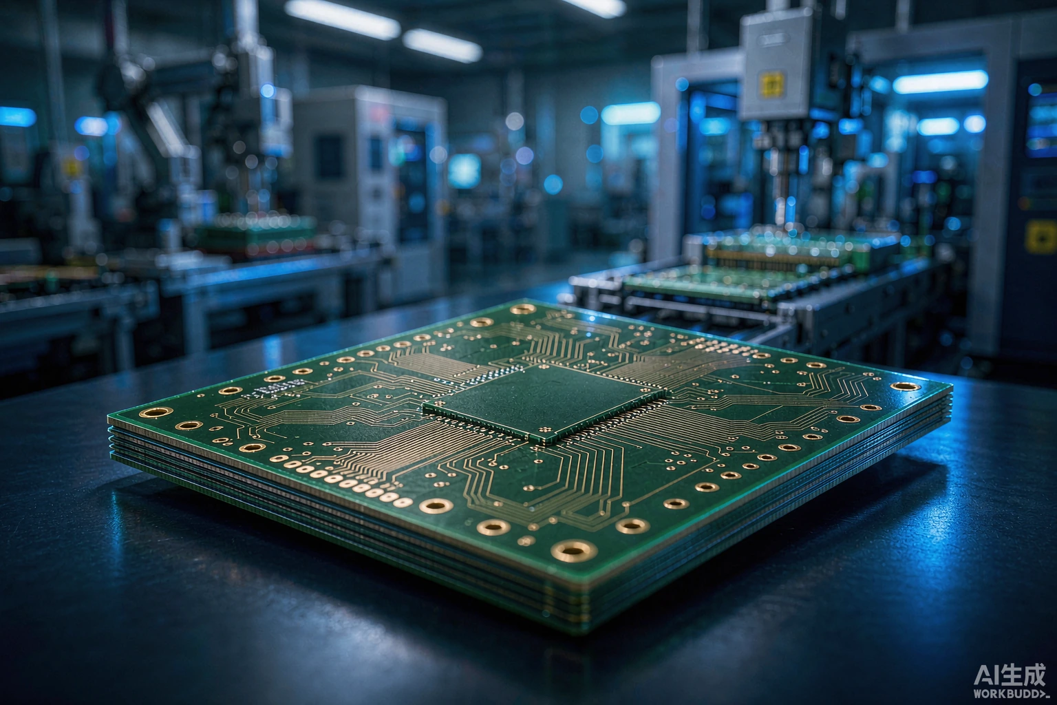
HDI PCB technology exists to solve a geometric problem: the components you have to route are smaller than the space left for the traces between them. A standard multilayer board escapes a 0.5 mm ball grid array with mechanical through-holes; at 0.4 mm pitch and below there is no room left for a hole between the pads. A high-density interconnect board replaces that hole with a laser-drilled microvia in a thin build-up layer, laminated on top of a conventional core, and recovers the routing space the through-hole used to consume.
This page is the technical reference for that decision. It covers what the stage number actually means, how the build-up layers are laminated and drilled, the microvia rules that decide whether a stackup is manufacturable, the design choices that move cost, and the capability limits we hold in production and on sample runs. Each parameter below is a production number, not a marketing range, and the shipped examples link to boards we have actually built.
Table of Contents
- What Is HDI PCB Technology?
- HDI Stages Explained: 1-Stage, 2-Stage, 3-Stage and Any-Layer
- How HDI PCB Technology Is Built: Sequential Lamination
- Laser Microvias: Hole Size, Aspect Ratio and Via Fill
- HDI Stackup Design: What to Control Before Release
- What Actually Drives HDI PCB Cost
- HDI vs Standard Multilayer: Which Build Fits
- Materials and Surface Finishes for HDI Boards
- Quality Control on HDI Builds
- Where HDI Boards Are Used
- How to Start an HDI Project With Season PCB
- Frequently Asked Questions
- Send the Stackup for Review Before You Commit to a Stage
What Is HDI PCB Technology?
HDI PCB technology describes an interconnection method, not a layer count. Three structural ideas separate an HDI board from a standard multilayer board: microvias drilled by laser instead of mechanically, build-up layers added by sequential lamination instead of one press cycle, and a routing density that lets a given net count fit into fewer or thinner layers than a through-hole design would need.
The practical effect is that a 6-layer HDI board can route what a 10-layer through-hole board routes, and can do it inside a 0.8 mm enclosure. That is why the format dominates smartphones, wearables, automotive camera and display modules, and any product where the mechanical envelope is fixed before the electrical design is finished.
These are the capability limits we hold on HDI builds. The sample column matters on prototypes, where the design is still being proven; the production column is what we can hold on a repeat order.
| Capability | Mass production | Sample runs |
|---|---|---|
| Layer count | 2 to 30 layers | 2 to 64 layers |
| Maximum HDI stages | 4+N+4 | Any-layer interconnect |
| Microvia diameter (minimum) | 4 mil (0.10 mm) | 3 mil (0.076 mm) |
| Mechanical drill (minimum) | 6 mil (0.15 mm) | 5 mil (0.127 mm) |
| Blind via aspect ratio | 1:1 | 1:1.2 |
| Through-hole aspect ratio | 12:1 | 20:1 |
| Inner layer line and space (minimum) | 2/2 mil | 1.8/1.8 mil |
| Outer layer line and space (minimum) | 2.5/2.5 mil | 2/2 mil |
| BGA pad (minimum) | 8 mil (0.20 mm) | 7 mil (0.18 mm) |
| Via to inner-layer trace (minimum) | 6 mil (0.15 mm) | 5 mil (0.127 mm) |
| Layer-to-layer alignment | 3 mil (0.076 mm) | 2 mil (0.05 mm) |
| Impedance tolerance | plus or minus 8% | plus or minus 5% |
| Finished thickness | 0.2 to 6.0 mm | 0.15 to 20 mm |
| Copper weight | 1/3 oz to 6 oz | 1/4 oz to 12 oz |
Two numbers in that table do most of the work. The blind via aspect ratio of 1:1 means a microvia may be as deep as it is wide, so a 0.10 mm via can only cross a dielectric around 0.10 mm thick. And the layer-to-layer alignment of 3 mil is the tolerance that decides how small a capture pad can be before registration starts eating the annular ring. If you are still weighing whether your design needs build-up layers at all, the stage comparison in our guide to 1-stage, 2-stage and 3-stage HDI works through that trade-off first.
HDI Stages Explained: 1-Stage, 2-Stage, 3-Stage and Any-Layer
A stage is one build-up lamination cycle on one side of the core, so a stackup written as i+N+i has i build-up layers above and below an N-layer core. A 1-stage board has one build-up layer per side, a 2-stage board has two, and any-layer means every adjacent layer pair is connected by microvias instead of only the outer pairs. The stage count is therefore a statement about how many times the panel is laminated, drilled and plated after the core is made, and every one of those cycles is a separate yield event.
These are the build-ups in current production, with a shipped example of each. The last column links to the actual board, which is the fastest way to compare a stackup against a design already running.
| Build-up | Total layers | Microvia structure | Typical use | Shipped example |
|---|---|---|---|---|
| 1+2+1 | 4 | One build-up layer per side | LED modules, simple wearables | 4-layer 1-stage irregular LED |
| 1+4+1 | 6 | One build-up layer per side over a 4-layer core | Automotive HUD and mirror modules | 6-layer automotive HUD |
| 1+10+1 | 12 | One build-up layer per side over a 10-layer core | Processor core boards, AI edge modules | 12-layer 1-stage core board |
| 2+2+2 | 6 | Two build-up layers per side over a 2-layer core | Audio boards, compact consumer devices | 6-layer 2-stage sound card |
| 2+4+2 | 8 | Two build-up layers per side over a 4-layer core | Dense control boards with impedance control | 6-layer 2-stage headphone |
| 2+6+2 | 10 | Two build-up layers per side over a 6-layer core | Industrial control, HDI prototypes | 10-layer 2-stage HDI prototype |
| 2+10+2 | 14 | Two build-up layers per side over a 10-layer core | High layer-count prototypes | 14-layer 2-stage HDI prototype |
| Any-layer | 10 | Microvias between every adjacent layer pair | Maximum density, sample runs | 10-layer HDI industrial control |
Inside a stage, the second-level microvia can land in one of two ways. In a staggered build, the second-stage via is offset and lands on its own pad on the first inner layer, which is easier to plate but spends routing space. In a stacked build, the second-stage via lands directly on top of the first, which saves space and is what makes 2-stage HDI worth its extra cycles, but it requires the first-stage via to be filled and planarised so the second laser drill does not open a void. Stacked vias are the reason filled via-in-pad, not the stage count, is often the real cost step in a 2-stage design.
How HDI PCB Technology Is Built: Sequential Lamination
The manufacturing side of HDI PCB technology is not a single lamination. The board starts as a conventional core, which is imaged, drilled and plated like any multilayer panel, and then build-up material is added one stage at a time. The sequence below is the production route for a 2-stage build.
- Image and etch the core layers, then laminate them into a sub-composite.
- Drill and plate the buried vias that connect the core layers.
- Laser-drill the first-stage microvias down to the first inner layer.
- Fill the microvias with conductive paste or copper, then planarise the surface.
- Laminate the second build-up layer and repeat the laser drilling and filling.
- Laminate the outer copper, then mechanically drill and plate the through-holes.
- Image the outer layers, apply solder mask and the selected surface finish, then route.
- Final inspection: electrical test, AOI, X-ray, microsection and TDR verification.
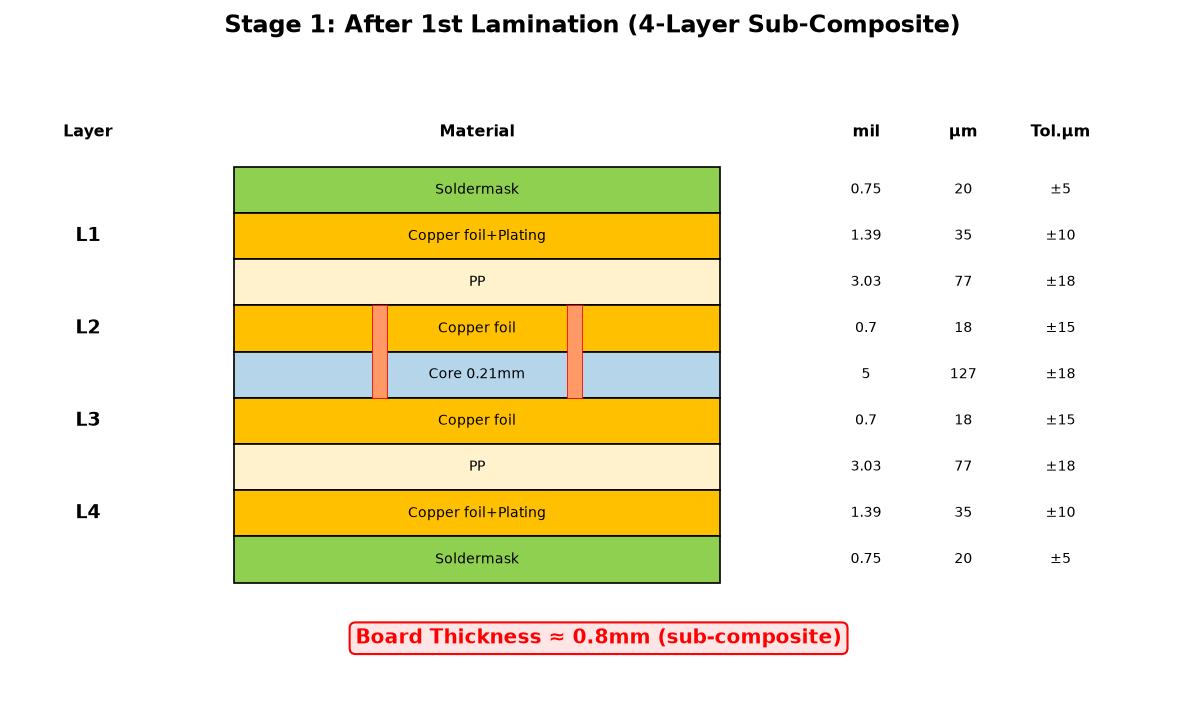
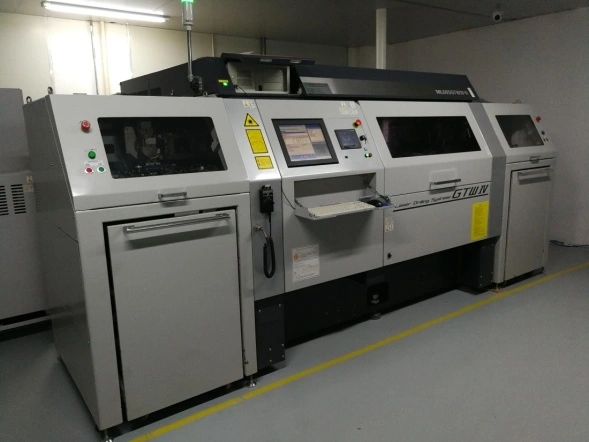
Two details in that sequence decide quality more than the process list suggests. First, the microvia fill has to be flat: any residual dimple becomes a void when the next layer is pressed over it, and a void under a second-stage via is not repairable after lamination. Second, the laser and mechanical drill programs must not share a queue. We run laser microvia drilling and mechanical drilling on separate dedicated lines, so an HDI panel does not wait behind standard through-hole work, and the drill specialists on each line only run one class of feature. That separation is not a scheduling nicety, it is what keeps a 0.10 mm via reproducible across a production lot.
Because the core is finished before the build-up starts, everything that happens in the core has to be right the first time. A buried via defect found after two build-up cycles means scrapping the whole panel rather than the core, which is why our CAM review treats core drilling and registration as the first checkpoint on an HDI job.
Laser Microvias: Hole Size, Aspect Ratio and Via Fill
Microvias are formed with CO2 laser drilling rather than a mechanical spindle, down to 0.10 mm in production and 0.076 mm on samples. What limits the geometry is not the laser spot but the aspect ratio: with a 1:1 blind via aspect ratio in production, a 0.10 mm microvia can only cross a dielectric roughly 0.10 mm thick. If your stackup needs a thicker build-up dielectric for impedance or mechanical reasons, the microvia has to grow with it, and the escape routing you were trying to gain is partly given back.
| Microvia structure | How it is built | Where it is needed | Design watch point |
|---|---|---|---|
| Single-level blind microvia | Laser-drilled through one build-up layer to the first inner layer | 1-stage HDI, both 1+2+1 and 1+4+1 builds | Depth-to-diameter ratio held at 1:1 |
| Stacked microvia | Second-stage via lands directly on the first-stage via pad | 2-stage and deeper builds where density is the limit | First-stage via must be filled and planarised |
| Staggered microvia | Second-stage via is offset and lands on a separate pad | The same builds when the plating window is tight | Consumes routing space on the first inner layer |
| Filled via-in-pad | Via is filled with conductive paste or copper, plated and planarised | Fine-pitch BGA and package-on-package devices | Fill quality verified by microsection on each lot |
| Buried via in the core | Mechanically drilled and plated before any build-up cycle | Any stackup needing core-to-core connection | Drilled before lamination, so defects are unrecoverable |
| Back-drilled through via | Controlled-depth drilling removes the unused plated stub | High-speed channels where stub resonance degrades the eye | Needs its own drill program and depth control |
| Cavity and edge plating | Controlled-depth routing plus selective plating on the edge | Modules where a component sits inside the board | Routed after lamination, so the stackup sets the depth |
Via-in-pad with conductive fill is the structure most often confused with HDI itself. It is a distinct process step: the via is filled, plated over and planarised so the BGA pad can be placed directly over it. It is what allows a 0.4 mm pitch array to escape without dog-bone fanout, and it is also one of the more expensive steps in the build, so it belongs under the BGA field rather than across the whole board. Back drilling follows the same logic at the other end of the design: it is a cost step you accept on high-speed channels, not a default finish on every through-hole.
HDI Stackup Design: What to Control Before Release
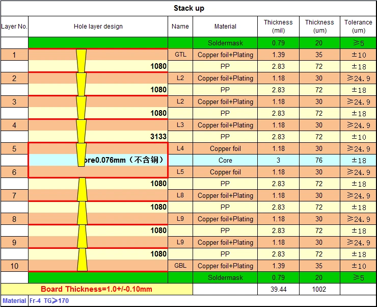
An HDI stackup is where the electrical and the mechanical requirements are forced to agree. Impedance is set by the dielectric thickness between the signal layer and its reference plane, but that same thickness is limited by the aspect ratio of the microvia that has to cross it. Copper balance decides whether the panel presses flat, and registration decides how small the capture pads can be. These are the items we check before a design goes to production, and the values we hold.
| Stackup item | What we hold to | Why it matters |
|---|---|---|
| Build-up symmetry | Same construction above and below the core | An unbalanced build-up warps across the lamination cycles |
| Dielectric thickness | Agreed against the impedance target before release | Sets impedance and caps the microvia depth at a 1:1 ratio |
| Layer-to-layer alignment | 3 mil (0.076 mm) production, 2 mil (0.05 mm) samples | Microvia capture pads and BGA escapes depend on registration |
| Via to inner-layer trace | 6 mil (0.15 mm) production, 5 mil (0.127 mm) samples | Prevents microvia breakout and CAF risk on thin dielectrics |
| Copper balance | Balanced copper distribution on every layer | Uneven copper causes resin starvation and thickness variation |
| Drill-to-copper registration | Verified in the drill program against the artwork | Biased registration closes the annular ring on a 0.20 mm pad |
| Panel utilisation | Stackup drawn to fit a standard production panel | A poor fit raises cost faster than any design rule |
This stackup review is where HDI PCB technology is applied as a service rather than as an order step. CAM engineers read the layer stack, the dielectric selection and the copper balances, then return an optimised proposal with simulated impedance values before production begins. Front-loading the stackup review is what keeps a project from being redesigned after the first article, when the tooling has already been paid for. The same review covers controlled impedance, where we hold plus or minus 8% in production and plus or minus 5% on samples, verified by TDR testing on every panel, for 50 ohm single-ended and 90 or 100 ohm differential structures.
What Actually Drives HDI PCB Cost
HDI PCB technology costs more than a through-hole multilayer board because each lamination cycle is a separate yield event, and because the fill, planarisation and microsection verification that make stacked vias reliable are real process steps. The useful way to read the table below is not as a price list but as a ranking of design decisions: the top two rows dominate everything else.
| Design decision | Cost direction | Why | How to pull it back |
|---|---|---|---|
| Each extra lamination cycle | Rises steeply | Separate yield, alignment and registration event | Move layers into the core instead of adding a stage |
| Any-layer interconnect | Rises steeply | Every layer pair needs its own microvia and fill step | Keep any-layer for samples and small volumes |
| Filled via-in-pad | Rises | Fill, planarisation and microsection verification | Apply it under the BGA field only |
| 2 mil inner line and space | Rises | Narrower etch window and lower imaging yield | Use it only where the ball pitch forces it |
| 0.076 mm microvias | Rises | Harder to drill, fill and plate reproducibly | Stay at 0.10 mm unless the pad pitch demands smaller |
| Tighter impedance tolerance | Rises | Narrower process window, more TDR review per lot | Design in margin instead of buying it from the process |
| Asymmetric stackup | Rises | Warpage needs extra process control to hold flat | Mirror the build-up above and below the core |
| Poor panel utilisation | Rises | The panel is consumed whether the space is used or not | Let CAM nest and rotate the array before the outline is frozen |
The honest summary is that HDI is worth its cost when it removes something: mechanical drill steps, layers, or board area. A 2-stage build that replaces a 12-layer through-hole stackup with an 8-layer HDI stackup is usually the cheaper board, not the more expensive one, once assembly yield and thickness are counted. HDI becomes expensive when it is used for density the product does not actually need, which is why we push the stage question back to the design team before quoting.
HDI vs Standard Multilayer: Which Build Fits
The decision is driven by the smallest feature the design has to escape, not by the layer count. If the finest ball pitch is 0.5 mm and there is room for a through-hole between the pads, a standard multilayer board is the cheaper answer and will have fewer process risks. HDI earns its place when the pitch drops below that, when the enclosure thickness is fixed, or when the layer count needed for a through-hole escape would push the board past the mechanical budget.
| Requirement | Standard multilayer | HDI build-up |
|---|---|---|
| Smallest ball pitch | 0.5 mm and above routes comfortably | 0.4 mm and below, with pads down to 0.20 mm in production |
| Via strategy | Mechanical through-holes and buried vias | Laser microvias plus buried and back-drilled vias |
| Routing the same net count | Needs more layers to escape the same ball count | Build-up layers carry the escape, so the core stays smaller |
| Minimum mechanical via | 6 mil (0.15 mm) | 4 mil (0.10 mm) microvia, 3 mil (0.076 mm) on samples |
| Thickness for a fixed enclosure | Limited by the core and prepreg build | Outer build-up is thin, so overall thickness comes down |
| Cost direction | Lower tooling when the routing fits | Higher per unit until it removes layers or drill steps |
| Best fit | Industrial, power, LED and automotive boards at coarse pitch | Dense, thin products in a fixed mechanical envelope |
Our process capability page lists both routes side by side, including the mechanical layers and the HDI PCB category where the current builds are collected. If the design sits on the boundary, send the Gerber data and the target pitch and we will quote both options rather than assume the denser one.
Materials and Surface Finishes for HDI Boards
Build-up layers are thin, so the laminate has to survive repeated press cycles without losing dimensional stability, and the surface finish has to sit on pads as small as 0.20 mm without bridging. We process FR-4 from Tg 130 to Tg 180, higher Tg grades such as IT-180A and S1000-2, low-loss materials including Megtron 6 and 7 and Tachyon 100G, Rogers RO4000 and RO3000 series laminates, and flexible polyimide. Material selection across that range covers applications from DC to 100 GHz.
For most HDI digital products the laminate choice is a thermal question, not an RF one: the number of lamination cycles a material can take matters more than its loss tangent. Where the board also carries a high-speed or RF channel, the dielectric decision moves to the loss budget, and the stackup may end up mixed, with a low-loss build-up over a conventional FR-4 core. Our PCB materials and laminates guide covers the selection criteria and the specific grades in more detail, and the Rogers high-frequency build shows a worked example with measured Dk and Df values.
Finishes available on HDI builds are ENIG, ENEPIG, OSP, HASL and lead-free HASL, immersion silver, immersion tin, and hard gold for edge contacts, with ENIG plus OSP as a combined option. For fine-pitch assembly ENIG or ENEPIG is the usual answer because the flat pad preserves coplanarity, while OSP suits high-volume reflow where the shelf life is managed. Hard gold is specified for gold-finger and press-fit interfaces rather than for solderable pads.
Quality Control on HDI Builds
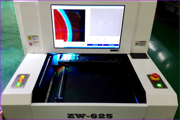
Every production batch passes 100% electrical test, AOI, X-ray inspection and TDR impedance verification. Beyond the electrical checks, microsection analysis confirms plating thickness and layer alignment on every lot, solderability testing validates the surface finish, and a documentation package with lot traceability ships with each order. On a build-up board the microsection is not a sampling formality: it is the only way to see whether a microvia filled completely and whether the dielectric opened during the multiple press cycles.
Production follows IPC-A-600 Class 2 as standard, with Class 3 acceptance available for high-reliability programs. Our processes are benchmarked against IPC-6012 for rigid boards and IPC-6018 for microwave boards, and the quality system is certified to ISO 9001:2015 and IATF 16949, with UL 796 recognition and cUL listing for the North American market, and RoHS and REACH compliance.
Where HDI Boards Are Used
The applications below all reach for HDI PCB technology for the same reason: the mechanical envelope is fixed before the electrical design is finished, so the routing has to fit the space rather than the other way round. These are the builds currently in production at our Shenzhen plant.
- Automotive display and camera modules: 6-layer HDI automotive HUD and 6-layer HDI rearview mirror boards, where the driver circuit sits behind the display.
- LED display and lighting: 6-layer HDI LED display and the 4-layer 1-stage irregular LED board with a non-rectangular outline.
- Wearables and audio: 1-stage smartwatch, 2-stage sound card and 2-stage headphone boards.
- Computing and control: 12-layer 1-stage core board for processor modules and 10-layer HDI industrial control for machine and drive electronics.
- Prototyping: 10-layer 2-stage and 14-layer 2-stage HDI prototype builds that validate a stackup before volume tooling.
How to Start an HDI Project With Season PCB
Send the Gerber or ODB++ data together with the stackup drawing, the impedance requirements and the target ball pitch. If the stage is still open, say so and include the enclosure thickness and the net count; the engineering team returns a comparison of the manufacturable options showing what each one does to the build-up and what process risks it carries. That assessment is part of our PCB manufacturing services, and it is done before quotation rather than after the order.
Samples and production run on the same data set, so a prototype stackup is not re-engineered for volume unless the design changes. For standard and compressed schedules, see our PCB lead time page. To see the broader manufacturing picture, the factory display covers the plant and the lines the HDI work runs on.
Frequently Asked Questions
What is the difference between HDI stages and layer count?
The stage number counts build-up lamination cycles per side, while the layer count is the total number of conductive layers. A 10-layer board can be built as 2+6+2 (two stages), 1+8+1 (one stage) or any-layer, and those options differ in cost and process risk even though the layer count is identical. What changes is how many times the panel is laminated and laser-drilled after the core is finished.
How do I know whether my design actually needs HDI?
Start with the smallest ball pitch and the escape routing. If a 0.5 mm or coarser array escapes comfortably with mechanical through-holes, a standard multilayer board is cheaper. HDI becomes necessary when the pitch drops to 0.4 mm and below, when the enclosure thickness is fixed, or when the layer count a through-hole escape needs would exceed the mechanical budget. Send the data and we will quote both routes instead of assuming the denser one.
What HDI stackups can you build in production?
In production, HDI PCB technology covers 2 to 30 layers with build-ups up to 4+N+4, and sample runs extend to 64 layers with any-layer interconnect. Sequential-lamination designs using stacked or staggered microvias are supported across that range, including builds with buried vias in the core and back-drilled through-holes.
What is your minimum microvia size and aspect ratio?
Microvias are laser-drilled down to 4 mil (0.10 mm) in production and 3 mil (0.076 mm) on samples, with a blind via aspect ratio of 1:1 in production and 1:1.2 on samples. Because the aspect ratio is 1:1, a 0.10 mm microvia can cross a dielectric about 0.10 mm thick, so build-up thickness and microvia size have to be chosen together rather than independently.
Which materials do you process for HDI boards?
FR-4 from Tg 130 to Tg 180, higher Tg grades such as IT-180A and S1000-2, low-loss materials including Megtron 6 and 7 and Tachyon 100G, Rogers RO4000 and RO3000 series laminates, and flexible polyimide. Halogen-free constructions are available with the S1150G grade at Tg 150 and above. Material selection across the range covers applications from DC to 100 GHz.
Can you hold controlled impedance on an HDI stackup?
Yes. Impedance is controlled to plus or minus 8% in production and plus or minus 5% on samples, covering 50 ohm single-ended and 90 or 100 ohm differential structures, with TDR testing on every panel. Impedance on a build-up board depends on the dielectric thickness between the signal layer and its reference plane, so the stackup and the impedance target are reviewed together before production.
Do you support via-in-pad and filled vias?
Via-in-pad and conductive via fill are both standard process options, along with controlled-depth drilling, cavity boards, back drilling, edge plating and in-board beveling. Filling quality is verified by microsection on each lot. We normally recommend keeping filled via-in-pad under the BGA field rather than across the whole board, because it is one of the more expensive steps in the build.
What files do you need to quote an HDI board?
Gerber or ODB++ data, a stackup drawing with dielectric thicknesses, the impedance requirements, the laminate callout, layer count and quantity. If the target ball pitch and the enclosure thickness are known, include them: they are the two inputs that decide whether a 1-stage, 2-stage or any-layer build is the right answer.
Send the Stackup for Review Before You Commit to a Stage
Send the Gerber data with the target ball pitch, layer count and quantity. The engineering team returns a per-stage assessment showing which HDI build is manufacturable, what each option does to the build-up and what process risk it carries, so the stage decision is made on data rather than on a default.
Data goes to szpcb@season-pcb.com, or through the contact page if you prefer a form. For an indicative starting point without waiting for a reply, the online quote page will take a first pass at pricing the stackup you describe.