Book Appointment Now

PCB Manufacturing Capability
PCB Process Capability Table
| Item | Mass Production | Sample |
|---|---|---|
| Material | FR4/Ordinary Tg /High Tg /PI/ Low-k/Lead Free/Halogen Free/High Frequency/High Speed | FR4/Ordinary Tg /High Tg /PI/ Low-k/Lead Free/Halogen Free/High Frequency/High Speed/Ceramic/Metal Base/Glass Substrate |
| Type | HDI/Multilayer/FPC/Rigid-Flex/High Frequency/High Speed/Hybrids & Mixed Dielectrics | HDI/Multilayer/FPC/Rigid-Flex/High Frequency/High Speed/Hybrids & Mixed Dielectrics |
| Layer | 2-30 | 2-64 |
| Max HDI Stages | 4+N+4 | Any layer Interconnect |
| PCB Thickness | 0.2-6.0mm | 0.15-20mm |
| Copper Weight | 1/3-6OZ | 1/4-12OZ |
| Mechanical Drill Size(Min) | 6mil(0.15mm) | 5mil(0.127mm) |
| Microvia Hole Size (Min) |
4mil(0.1mm) | 3mil(0.076mm) |
| Trace width/Spacing(Min) | Inner layer 2/2mil, Outer layer 2.5/2.5mil | Inner layer 1.8/1.8mil, Outer layer 2/2mil |
| Panel Size (Max) |
800*600mm | 1050*610mm |
| Outline Tolerance (Min) |
±3mil(0.076mm) | 2mil(0.05mm) |
| BGA Pad (Min) |
8mil(0.2mm) | 7mil(0.18mm) |
| Through-Hole Aspect Ratio | 12:1 | 20:1 |
| Blind Via Aspect Ratio | 1:1 | 1:1.2 |
| Impedance Tolerance (Min) |
8%(Single-ended, Differential) | 5%(Single-ended, Differential) |
| Via to Inner Layer Trace Spacing (Min) |
6mil(0.15mm) | 5mil(0.127mm) |
| Level to Level Alignment (Min) |
3mil(0.076mm) | 2mil(0.05mm) |
| Special Process | VIP /Conductive Via Fill /Controlled Depth Drill and Rout/Cavity Boards /Back Drilling/Edge Plating/In‐board Beveling | VIP /Conductive Via Fill /Controlled Depth Drill and Rout/Cavity Boards /Back Drilling/Edge Plating/In‐board Beveling/Buried Capacitance |
| Surface Finishes | ENIG/OSP/HASL/Electric Gold Finger/Electric Hard Gold/Immersion Silver/Immersion Tin/ENIG+OSP/ENEPIG | ENIG/OSP/HASL/Electric Gold Finger/Electric Hard Gold/Immersion Silver/Immersion Tin/ENIG+OSP/ENEPIG |
Advanced Manufacturing Capability
Season PCB operates a wide range of manufacturing technologies and process specifications designed to meet the demanding requirements of modern electronics. Our state-of-the-art facility in Shenzhen, China, is equipped with advanced equipment for HDI, multi-layer, high-frequency, and high-speed PCB production, making us a trusted partner for engineers worldwide.
Core Capability Specifications
Layer Count Capability
We produce from 2 to 30 layers in volume production, with sample capability up to 64 layers, including any-layer HDI constructions. Whether you need a simple double-sided board or a complex multilayer backplane, every layer is aligned with precise layer-to-layer registration.
Fine Line Capability
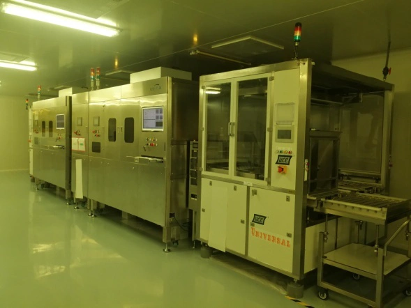
We achieve minimum trace width and spacing of 0.05mm/0.05mm (2mil/2mil) using LDI (Laser Direct Imaging) technology. This fine-line capability enables high-density routing for advanced IC packages and fine-pitch BGA designs.
Impedance Control Capability
We deliver precise impedance control with tolerance of plus or minus 8% or better. We support single-ended 50 ohm, differential 100 ohm and 90 ohm, and custom impedance requirements, verified by TDR testing on every panel.
Behind these numbers is a stackup engineering service: our CAM engineers review your layer stack, dielectric selection, and copper balances, then return an optimized proposal with simulated impedance values before production begins. This front-loading avoids mid-project redesigns and shortens the path from design handoff to first article.
Material Capability
We process FR-4 (Tg130 to Tg180), high-Tg materials (IT-180A, S1000-2), low-loss materials (Megtron 6/7, Tachyon 100G), Rogers RO4000 and RO3000 series, and flexible polyimide materials. This material versatility supports frequencies from DC to 100GHz.
Surface Finish Capability
We offer ENIG, ENIPIG, HASL, Lead-free HASL, OSP, Immersion Silver, Immersion Tin, and Hard Gold surface finishes. Our engineering team recommends the proper surface finish for each application’s solderability, shelf life, and contact requirements.
Contact Season PCB to discuss your specific requirements. Our engineering team will review your design files and confirm feasibility before quotation.
Our via technologies also cover through-hole, blind via, buried via, and any-layer microvia. This comprehensive portfolio supports complex HDI designs with high interconnection density.
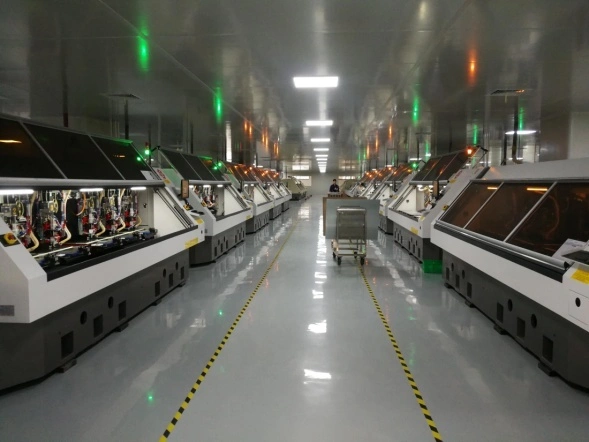
Drilling capability matches the stack: mechanical spindle drilling down to 0.15mm with aspect ratios up to 12:1 in production, CO2 laser drilling for 0.1mm microvias, and controlled-depth drilling for back-drilled structures. Laser and mechanical drilling run on separate dedicated lines, so HDI microvia panels never queue behind standard through-hole work.
Testing and Quality Assurance
Every production batch passes comprehensive testing: 100% electrical testing, AOI inspection, X-ray inspection, and TDR impedance testing. These testing capabilities ensure every PCB meets our quality standards and customer specifications.
Quality assurance extends beyond electrical checks: microsection analysis confirms plating thickness and layer alignment on every production lot, solderability testing validates surface finish shelf life, and documentation packages with lot traceability ship with each order. Production follows IPC-A-600 Class 2 as standard, with Class 3 acceptance available for high-reliability programs.
Our PCB manufacturing capability is continuously upgraded to meet evolving industry demands. Season PCB invests in advanced equipment and engineer training every year, ensuring we can handle your most challenging designs. Contact our engineering team to discuss how we can support your next project.
Our processes are benchmarked against IPC standards including IPC-6012 for rigid PCBs and IPC-6018 for microwave boards. These standards define the quality and capability levels that our production consistently meets.
For more information about our manufacturing facility, visit our factory display page. To see our complete product range, browse PCB products. Learn about our PCB lead time for production planning.
Frequently Asked Questions
What layer count and HDI stages can you build?
Volume production covers 2 to 30 layers, while sample runs go up to 64 layers. HDI constructions reach 4+N+4 stages in production and any-layer interconnect for samples, so sequential-lamination designs with stacked or staggered microvias are fully supported.
What is your minimum trace width and spacing?
Production panels hold 2mil/2mil (0.05mm) line and space using LDI imaging; sample capability extends to 1.8mil/1.8mil on inner layers. These geometries support fine-pitch BGA, advanced IC substrates, and high-density routing.
What impedance tolerances can you hold?
Single-ended and differential impedances are controlled to plus or minus 8% in production and plus or minus 5% on samples, covering 50 ohm single-ended and 90 or 100 ohm differential structures. Every panel is verified by TDR testing before shipment.
Which laminate materials do you support?
We process FR-4 from Tg130 to Tg180, high-Tg and low-loss materials such as IT-180A, S1000-2, Megtron 6/7, and Tachyon 100G, Rogers RO4000 and RO3000 series, and flexible polyimide. Material selection covers applications from DC to 100GHz.
What surface finishes are available?
Available finishes include ENIG, ENEPIG, OSP, lead-free HASL, immersion silver, immersion tin, electrolytic hard gold, gold fingers, and combined ENIG+OSP. We recommend the finish that matches your solderability, wire-bonding, and shelf-life requirements.
How do I get a DFM review and quotation?
Send your Gerber files and stackup requirements through our contact page or quote form. Our engineers run a free DFM review covering drill-to-copper, annular ring, and impedance feasibility, and a quotation is typically returned within 24 hours.