Book Appointment Now

PCB materials and laminates from FR4 to Rogers: Tg grades, halogen-free options, Dk and Df, copper weight and the criteria that decide the choice.
PCB Materials and Laminates: How to Choose the Right Substrate
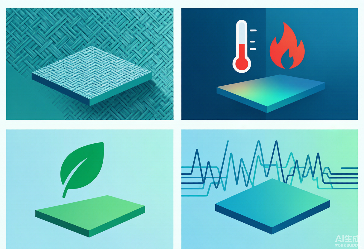
PCB materials decide more of the finished board than any other single choice. The laminate sets the dielectric constant that fixes trace width for a target impedance, the dissipation factor that decides insertion loss, the glass transition temperature that decides how many times the board can be reflowed, and a large part of what the board ultimately costs. A stackup that is perfect on paper fails if the grade behind it cannot survive the assembly profile.
This page is the reference for that choice. It covers the laminate families we process and the grades within them, what Tg, Dk and Df actually predict, when a halogen-free or low-loss material is worth its price step, how copper weight interacts with fine-line geometry, and what belongs on a drawing when the material has to be specified unambiguously. Every grade and every number below is something we run; where a value depends on the supplier datasheet, the page says so instead of quoting a figure.
Table of Contents
- What Are PCB Materials and Laminates?
- The Laminate Families We Process
- Tg, Decomposition Temperature and Thermal Stress
- Halogen-Free Laminate: When It Matters
- Dk and Df: How the Laminate Sets High-Speed Performance
- Copper Weight, Current and Fine Lines
- PCB Materials Selection: Matching the Grade to the Requirement
- Mixed Dielectric and Hybrid Stackups
- What Material Choice Does to Cost
- Laminate Quality, Traceability and Certification
- How to Specify PCB Materials on a Drawing
- Frequently Asked Questions
- Get the Material and Stackup Reviewed Together
What Are PCB Materials and Laminates?
A rigid laminate is a composite: woven glass reinforcement, a resin system, and copper foil on one or both faces. The resin decides the thermal behaviour and the electrical loss, the glass style decides mechanical stiffness and dimensional stability, and the copper decides current capacity as well as how fine the traces can be etched. Change any one of those and the same gerber data produces a different board.
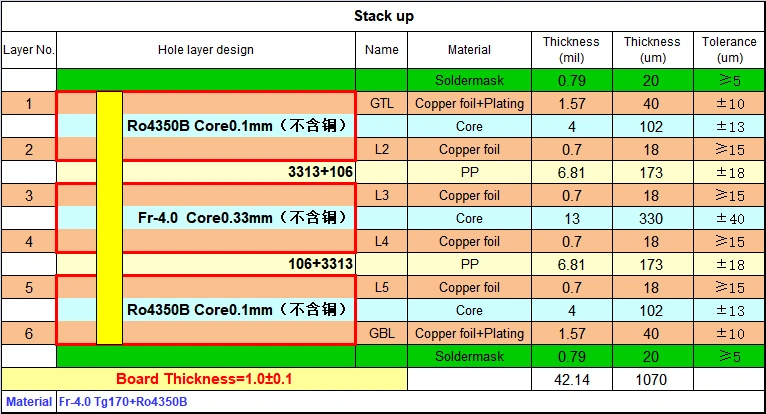
Boards are then built from two forms of the same material system. A core is a laminate with copper already bonded on both sides, so it forms a finished inner layer. Prepreg is the same resin and glass in a semi-cured state: it becomes the bonding layer, and it is what fills the space between cores during lamination. The stackup drawing is essentially a list of cores and prepregs, with the finished dielectric thickness of each.
That is why material selection on a multilayer board is a stackup exercise rather than a shopping decision. Prepreg flows under heat and pressure, so its cured thickness depends on the copper it has to fill; the dielectric thickness that comes out of the press is what the impedance calculation has to use. On build-up boards the same logic applies to the outer layers, where the build-up dielectric is also capped by the aspect ratio of the microvias that cross it, as covered in our HDI PCB technology reference.
The Laminate Families We Process
Materials group by the thermal and electrical job they do, not by brand. The table below lists the families we run, the grades within them, and where each family earns its place. Where a Tg value depends on the specific grade rather than on the family, the table says so: quoting a single number for a whole family is how material mistakes start.
| Family | Grades we process | Tg | Where it fits |
|---|---|---|---|
| Standard FR-4 | General-purpose FR-4 | Tg 130 to Tg 150 | Thin consumer and industrial boards with a normal reflow profile |
| Mid-Tg FR-4 | S1000H | Tg 150 | Volume digital boards where lead-free assembly is the main thermal load |
| High Tg FR-4 | S1170G, IT-180A, S1000-2 | Tg 170 to Tg 180 | Thick multilayer boards, repeated reflow, high layer counts |
| Halogen-free FR-4 | S1150G | Tg 150 and above | Programs that carry a halogen-free material restriction |
| Low-loss | Megtron 6, Megtron 7, Tachyon 100G | Per grade datasheet | High-speed digital channels where insertion loss decides the link |
| PTFE and hydrocarbon | Rogers RO4000 and RO3000 series | Per grade datasheet | RF, microwave, antenna and radar front-end designs |
| Polyimide | Flexible polyimide | Per grade datasheet | Flex and rigid-flex builds that must survive soldering and bending |
Two entries in that table are easy to confuse. S1000H is a Mid-Tg material at Tg 150, which is the right answer for a large share of volume digital work: it is not a High Tg grade, and it is not a halogen-free grade either. Where a program needs either of those properties, the callout has to change to a different grade rather than an option on the same one. S1170G at Tg 170 and S1000-2 at Tg 180 are the High Tg route, and S1150G is the halogen-free route.
We process FR-4 from Tg 130 to Tg 180, the High Tg and low-loss materials listed above, Rogers RO4000 and RO3000 series laminates and flexible polyimide, which together covers applications from DC to 100 GHz. Copper weight runs from 1/3 oz to 6 oz in production and 1/4 oz to 12 oz on samples, and finished thickness from 0.2 mm to 6.0 mm in production with 0.15 mm to 20 mm available on samples. The full matrix is published on our process capability page.
Tg, Decomposition Temperature and Thermal Stress
In PCB materials the glass transition temperature is where the resin stops behaving like a rigid solid and starts behaving like a soft one. Above Tg the material expands much faster with temperature, so the z-axis expansion that a plated barrel has to survive during reflow grows sharply. That is the mechanism behind Tg selection: it is not about the operating temperature of the product, it is about the assembly thermal cycles and the number of lamination presses the panel has to survive before it is even assembled.
Tg alone is a weak predictor on thick boards. Two materials with the same Tg can behave very differently at 260 degrees, because what fails first is usually delamination at the resin and glass interface, not the glass transition itself. The parameters that predict that better are the decomposition temperature, the time to delamination at a fixed temperature, and the z-axis coefficient of thermal expansion. All three are datasheet values, and all three should be compared at the thickness you are actually building, not at the 1.6 mm test coupon.
For HDI work there is a second thermal constraint that does not appear on a standard datasheet table: the number of lamination cycles the material tolerates. A 2-stage build presses the panel through several cycles, each one a thermal excursion on material that has already been cured once. That is why build-up work tends to sit at Tg 150 and above even when the finished product never sees a high temperature, and why the stackup review happens against the material choice rather than after it.
Halogen-Free Laminate: When It Matters
Halogen-free means the resin system does not use a brominated flame retardant. Manufacturers reach the same flammability requirement with phosphorus and nitrogen chemistry instead, which changes the resin formulation, the curing behaviour and the price. It is a material callout, not a process option: you cannot make a standard grade halogen-free by treating it differently.
Our halogen-free grade is S1150G, rated Tg 150 and above. It is specified when a customer compliance requirement, an end-market restriction or an internal material declaration demands it. One distinction matters when reading a drawing: a standard Mid-Tg FR-4 such as S1000H uses a brominated flame retardant system. Halogen-free is a different grade, not an option on that one. If a drawing calls for halogen-free and also names a standard grade, that is a contradiction to resolve before quotation rather than during production.
The practical question is whether the requirement is real. Halogen-free matters when the finished product is subject to a material declaration, when the customer has written it into the specification, or when the product is disposed of under a regime that restricts halogenated flame retardants. Where none of those apply, the same thermal and electrical performance is usually available at a lower material step, and the stackup review will say so.
Dk and Df: How the Laminate Sets High-Speed Performance
Dk and Df are the two PCB materials parameters that decide high-speed behaviour. The dielectric constant sets the capacitance per unit length of a trace, which is why it fixes the trace width needed for a target impedance. The dissipation factor (Df) sets how much energy the dielectric absorbs, which is why it drives insertion loss and rise-time degradation. Both are measured at a stated frequency, and a value quoted without that frequency is not comparable with anything: Dk and Df both move with frequency, and material datasheets quote them at whichever test frequency the supplier chose.
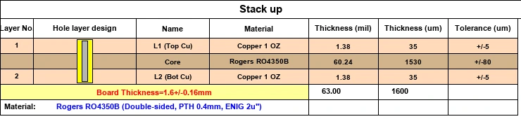
A worked example from our own production makes the point. The Rogers RO4350B build is specified at Dk 3.48 plus or minus 0.05 and Df 0.0037, both at 10 GHz. Those numbers come measured rather than nominal, and they are what the impedance simulation is run against. On a low-loss build the same discipline applies: the stackup is simulated with the datasheet values at the channel frequency, and the impedance tolerance we hold is plus or minus 8% in production and plus or minus 5% on samples, verified by TDR on every panel.
| Datasheet parameter | What it decides | What to check before specifying |
|---|---|---|
| Dk at a stated frequency | Trace width for a target impedance | Compare at the frequency the channel runs at, not at the supplier test frequency |
| Df at a stated frequency | Insertion loss and rise-time degradation | Same frequency discipline as Dk |
| Dk tolerance | How much impedance spread the material contributes | A tight Dk tolerance buys process margin |
| Tg | The assembly thermal window | Match it to the reflow cycles and the layer count |
| Decomposition temperature | The upper thermal limit before the resin degrades | Relevant for heavy copper and repeated lamination |
| Time to delamination at fixed temperature | Resistance to delamination under thermal stress | A better predictor than Tg alone on thick boards |
| CTE in x, y and z | Dimensional change with temperature | Z-axis CTE drives plated barrel cracking on thick boards |
| Copper foil weight and type | Current capacity, etchability and impedance | Heavy copper and fine lines compete for the same process window |
Copper Weight, Current and Fine Lines
Copper weight is specified in ounces per square foot, where 1 oz corresponds to roughly 35 microns of finished copper. We run 1/3 oz to 6 oz in production and 1/4 oz to 12 oz on samples, which spans everything from fine-line digital routing on 1/3 oz to heavy-current planes and bus bars on 6 oz.
The interaction that catches designs out when specifying PCB materials is the one between weight and line width. Heavier copper needs a wider etch window, because the same etching time that clears a thin foil will undercut a thick one. A design that specifies 6 oz copper and 3 mil traces is asking the process for two things that pull against each other, and the resolution is usually to keep heavy copper on the plane layers and fine lines on the signal layers rather than trying to do both on the same layer.
Copper weight also moves impedance, for a reason that is easy to miss: part of the current in a high-frequency trace travels in the conductor surface, so the effective thickness of the copper changes the inductance of the trace. When a stackup is simulated, the copper thickness is an input alongside the dielectric thickness. On inner layers we hold 2/2 mil line and space in production and 1.8/1.8 mil on samples, and on outer layers 2.5/2.5 mil in production and 2/2 mil on samples.
PCB Materials Selection: Matching the Grade to the Requirement
Selection becomes simple once the requirement is stated as a constraint rather than as a preference. The table maps the constraints we see most often onto the grade that satisfies them. Where two constraints conflict, for example a halogen-free restriction together with a Tg 180 requirement, the honest answer is that a different grade is needed rather than a compromise on the same one.
| Requirement | Grade to specify | Why that grade |
|---|---|---|
| Standard lead-free assembly, cost sensitive | Standard FR-4 at Tg 130 to Tg 150 | The thermal load is a single reflow and the board is thin |
| Repeated reflow, thick board, many layers | High Tg FR-4 such as S1170G (Tg 170) or S1000-2 (Tg 180) | Dimensional stability through multiple press and reflow cycles |
| Halogen-free restriction from the customer | S1150G at Tg 150 and above | The restriction is a material callout, not a process option |
| High-speed serial channels | Low-loss materials such as Megtron 6 or Megtron 7 | A lower dissipation factor reduces insertion loss at the same geometry |
| RF, microwave, antenna | Rogers RO4000 or RO3000 series | Stable Dk across frequency with a tight Dk tolerance |
| Flex or rigid-flex construction | Polyimide | Survives soldering and repeated flexing |
| Mixed RF and digital in one board | Hybrid stackup: low-loss build-up over an FR-4 core | Spends the loss budget only on the layers that carry RF |
| Tight impedance tolerance | A grade with tight Dk tolerance, simulated before release | Half of the impedance spread can come from the material itself |
One habit is worth building regardless of which grade comes out of the table: specify the requirement, not just the brand. A drawing that says only a supplier grade name leaves the process engineer guessing about the thermal and loss constraints behind it, and if that grade is unavailable, there is no way to judge a substitute. Naming the requirement alongside the grade is what makes a substitution reviewable.
Mixed Dielectric and Hybrid Stackups
A hybrid stackup puts a low-loss laminate where the RF or high-speed channels run and standard FR-4 everywhere else. It is the standard answer to the board that has one 10 GHz front end and a large digital section, because the loss budget is only spent on the few layers that need it. The optical module build is a working example: a Rogers layer set against FR-4 in a single stackup, with the impedance-controlled layers simulated separately from the digital ones.
Hybrid builds are not simply two boards pressed together, and the design work is in the interfaces. The two material systems expand at different rates, so the stackup has to be balanced around the centre line to keep the panel flat. Bonding a hydrocarbon or PTFE material to epoxy requires surface preparation that a pure FR-4 build does not, and the drill parameters have to suit the harder material wherever the hole passes through both. Where the RF layer is thin and the digital core is thick, the registration budget is set by the worst layer, not the average.
The payoff is usually worth it. A hybrid board that keeps RF performance while leaving 90% of the stack on FR-4 costs a fraction of an all-RF design, and it keeps access to the finishes, drill sizes and layer counts that standard processing already covers well. Our high-frequency builds collect the current examples.
What Material Choice Does to Cost
Material is one line in the cost structure, and it is rarely the largest: layer count, panel utilisation and the number of process steps usually outrank it, as set out in our breakdown of PCB cost components. What the material does do is change the process route, and process changes are where the real steps come from. The table below gives direction only, in relative terms, because an absolute comparison would depend on the stackup and the quantity.
| Material decision | Cost direction | Why |
|---|---|---|
| Standard FR-4 at Tg 130 to Tg 150 | Baseline | Broad availability and a wide process window |
| Mid-Tg FR-4 at Tg 150 | Small step up | A higher material price on the same process route |
| High Tg FR-4 at Tg 170 to Tg 180 | Moderate step up | Higher resin cost and a narrower lamination window on thick builds |
| Halogen-free FR-4 | Moderate step up | Phosphorus and nitrogen systems cost more than brominated resin |
| Low-loss laminate | Significant step up | Material price plus tighter control of the stackup and the press cycle |
| PTFE and hydrocarbon laminates | Largest material step | Special surface preparation and dedicated drill parameters |
| Polyimide | High | Film and adhesive systems with longer press cycles |
| Copper above 2 oz | Rises with weight | Etching and plating take longer and lose yield |
| Hybrid or mixed dielectric stackup | Rises | Two material systems and more lamination steps |
The useful conclusion is that over-specifying PCB materials is expensive in a way that is invisible on the drawing. A low-loss laminate specified because the product has one high-speed interface, applied to all layers, adds cost to every layer of the board. Naming the constraint instead of the grade lets the stackup put the expensive material where the loss budget actually is.
Laminate Quality, Traceability and Certification
Material performance is only as good as the process that bonds it. Every production batch passes 100% electrical test, AOI and X-ray inspection, with microsection analysis confirming plating thickness and layer alignment on each lot. Microsection is where laminate problems show up: resin starvation on a heavy-copper layer, voids under a build-up, or delamination at a glass bundle, none of which an electrical test sees.
Incoming material is handled the way the finished board is, with lot traceability through the process so that a material question can be traced back to a specific batch. Production follows IPC-A-600 Class 2 as standard, with Class 3 acceptance available for high-reliability programs, and the processes are benchmarked against IPC-6012 for rigid boards. The quality system is certified to ISO 9001:2015 and IATF 16949, with UL 796 recognition and cUL listing for the North American market, and RoHS and REACH compliance.
For programs that need it, material certification documents travel with the shipment, and the laminate supplier datasheet for the grade actually used can be provided on request. That last point matters on a hybrid stackup, where the datasheet that ships has to match the material in the press rather than the material in the original quotation.
How to Specify PCB Materials on a Drawing
Specifying PCB materials so that the callout cannot be misread takes five items:
- The laminate grade and its Tg, for example a High Tg FR-4 at Tg 170 or S1150G at Tg 150 and above for a halogen-free requirement.
- The requirement behind the choice, so a substitution can be judged rather than guessed.
- The stackup drawing, with the finished dielectric thickness of each layer rather than the raw prepreg specification.
- The copper weight per layer, and the line and space minimums the design actually needs.
- The impedance targets and the test frequency, plus the surface finish, since the finish sits on the same pads the impedance coupon is measured from.
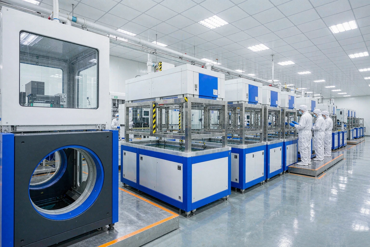
Send those five items with the gerber or ODB++ data and the review can start immediately. Where the material choice is still open, the engineering team will return a comparison of the grades that satisfy the constraints, including what each one does to the process route. Standard and compressed schedules are published on the PCB lead time page, and the broader manufacturing picture is on the factory display.
Frequently Asked Questions
What is the difference between a core and a prepreg?
A core is a laminate with copper foil already bonded to both faces, so it becomes a finished inner layer of the board. Prepreg is the same resin and glass in a semi-cured state: it has no copper, it flows under heat and pressure, and it bonds the cores together. A stackup is a list of cores and prepregs with the finished dielectric thickness of each, and that finished thickness is what the impedance calculation uses.
How do I choose between Tg 150, 170 and 180 laminates?
Choose by the thermal load the board has to survive, not by the product operating temperature. A single lead-free reflow on a thin board is comfortably served by Tg 150. Repeated reflow, thick boards and high layer counts push toward Tg 170 or Tg 180, because z-axis expansion above Tg is what stresses plated barrels and causes delamination. On build-up boards the number of lamination presses the material tolerates matters as much as the assembly profile.
Which laminate grades are halogen-free?
Halogen-free is a grade callout rather than a property of standard FR-4. The grade we process is S1150G, rated Tg 150 and above, which reaches the flammability requirement with phosphorus and nitrogen chemistry instead of a brominated flame retardant. If a customer specification or an end-market material declaration requires it, that grade belongs on the drawing instead of a standard FR-4 callout.
Do low-loss materials need a different stackup?
They need the same stackup discipline with tighter inputs. Dk and Df are frequency dependent, so the simulation has to use the datasheet values at the frequency the channel actually runs at, and the Dk tolerance of the grade becomes part of the impedance budget. Because the dielectric thickness between a signal layer and its reference plane drives most of the impedance, the stackup is usually adjusted rather than the design.
What Dk and Df values can you work to?
We design to the datasheet of the grade you specify, at the frequency your channel runs at, and we process material covering applications from DC to 100 GHz. A worked production example is the Rogers RO4350B build specified at Dk 3.48 plus or minus 0.05 and Df 0.0037, both at 10 GHz. Impedance is controlled to plus or minus 8% in production and plus or minus 5% on samples, verified by TDR on every panel.
Can you mix a high-frequency laminate with FR-4 in one stackup?
Yes, and it is often the cheapest way to keep RF performance without paying for a low-loss material on every layer. The design work is at the interfaces: the stackup is balanced around the centre line because the two materials expand at different rates, bonding a hydrocarbon or PTFE layer to epoxy needs its own surface preparation, and the registration budget is set by the worst layer rather than the average.
How does copper weight affect the design?
Copper weight sets current capacity, but it also narrows the etch window: the same etching that clears a thin foil will undercut a thick one, so heavy copper and fine lines pull against each other. We run 1/3 oz to 6 oz in production and 1/4 oz to 12 oz on samples. Copper thickness is also an input to the impedance simulation, because at high frequency part of the current travels in the conductor surface.
What should be on the drawing when specifying materials?
The laminate grade and its Tg, the requirement behind the choice so a substitution can be judged, the stackup drawing with finished dielectric thicknesses, the copper weight per layer with the line and space minimums, and the impedance targets with the test frequency and surface finish. Send those with the gerber or ODB++ data and the material review can start without a round of questions.
Get the Material and Stackup Reviewed Together
Send the gerber or ODB++ data with the thermal, loss and compliance constraints your product has to meet. The engineering team returns a material comparison and an optimized stackup with simulated impedance values, so the grade is chosen against the constraints rather than against a default.
Data goes to szpcb@season-pcb.com, or through the contact page if you prefer a form. For an indicative starting point, the online quote page will take a first pass at the stackup you describe.