Book Appointment Now

4-Layer 1-Stage HDI Irregular LED Display PCB
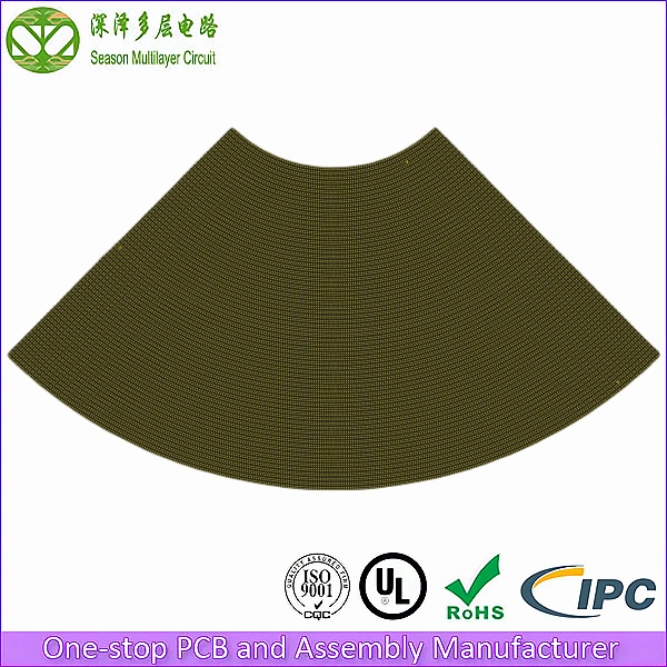
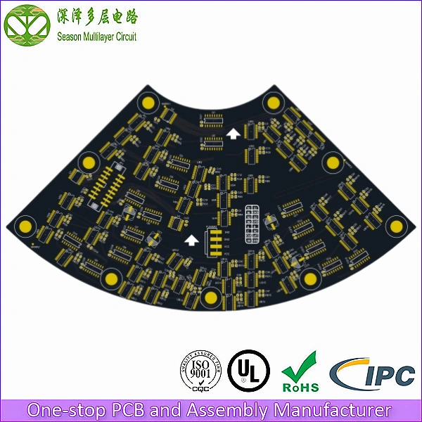
4-Layer 1-Stage HDI irregular LED display PCB built on a 1+2+1 structure with 0.10 mm laser blind vias, 4/4 mil fine-line routing, and a slim 0.6 mm FR4 Tg150 profile – engineered for P1.5625 fine-pitch creative LED screens and shipped from prototype to mass production by Season PCB.
Built on a 1+2+1 single-sequential-lamination build-up, the board routes the dense P1.5625 pixel field with 0.10 mm laser blind vias and 0.25 mm buried vias instead of through-holes, keeping the 234.9 x 130.4 mm panel flat with a symmetric 0.6 mm FR4 Tg150 stack. Season PCB has shipped HDI LED display boards for irregular and creative screen projects since 2018.
- 1+2+1 single-sequential-lamination HDI architecture – HDI density at close to standard 4-layer cost
- 0.10 mm laser blind vias free the P1.5625 pixel field from through-hole routing shadows
- OSP finish for low-cost, high-yield LED & driver SMT; custom irregular outlines routed to spec
- Free DFM review on every quote – prototype samples in 5-7 working days
1+2+1
1-Stage HDI Build
0.10 mm
Min Blind Via
4 / 4 mil
Min Line/Space
0.6 mm
Board Thickness
P1.56
Pixel Pitch
UL Listed
IPC-A-600 Class 2/3
ISO 9001:2015
IATF 16949
RoHS / REACH
100% E-Test
4-Layer 1-Stage HDI Irregular LED Display PCB Stackup Diagram (1+2+1)
The 1+2+1 stackup is the most cost-effective HDI architecture for fine-pitch LED display modules. Two sequentially laminated sub-layers carry the pixel-driving network, while the buried core handles power distribution and control signals:
- L1 / L4 (Outer Layers – 1 OZ Copper): The two outer layers carry the LED pad array and driver IC connections, finished at 1 OZ copper with OSP protection for low-cost, high-solderability SMT assembly.
- L2 / L3 (Buried Routing Core – 1 OZ Copper): L2 and L3 form the buried routing core, carrying the dense P1.5625 scan-line and current-return network on 4/4 mil traces.
- L1-L2 and L4-L3 Stage-1 Blind Micro-Vias: L1-L2 and L4-L3 laser blind vias at 0.10 mm connect the outer layers to the buried core without consuming surface routing channels – critical under 0402 and smaller LED packages.
- L2-L3 Buried Via Window: The L2-L3 buried via window at 0.25 mm jumps the central core, shortening power and ground paths between the two routing layers.
- FR4 Tg150 Base Material: FR4 Tg150 base material keeps the 0.6 mm panel flat and dimensionally stable through multiple lead-free reflow cycles.
- Symmetric 1+2+1 Stack for Warpage Control: The symmetric 1+2+1 build is balanced around the core centerline, minimizing warpage on large 234.9 x 130.4 mm display panels.
- Single Sequential Lamination Cycle: A single sequential lamination cycle keeps cost and lead time close to a standard 4-layer board while delivering full HDI routing density.
- 0.6 mm Finished Thickness for Lightweight Modules: The 0.6 mm finished thickness reduces module weight – a key advantage for curved and suspended irregular display installations.
- Tuned for P1.5625 Fine-Pitch LED Routing: Stackup is fully customizable: copper weights, prepreg selections, and impedance targets are tuned to your specific LED module design.
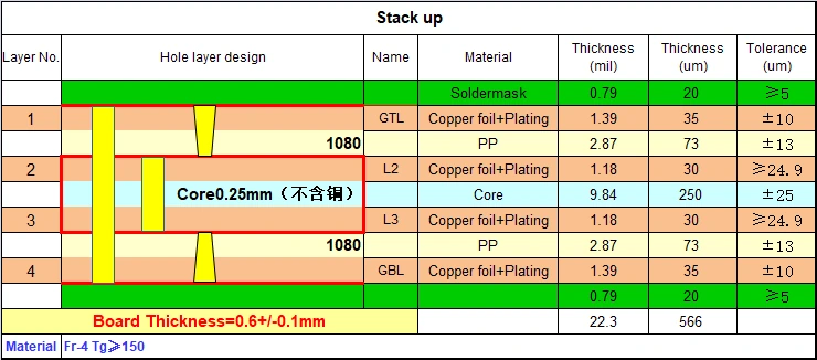
This 1+2+1 stackup is a production-proven reference for fine-pitch LED display modules on FR4 Tg150. Our engineering team tunes prepreg selection, copper weight, and via diameters to your pixel pitch, outline geometry, and impedance targets – all in a single sequential lamination cycle for the lowest possible HDI cost on fine-pitch LED display boards.
Technical Capability & Specifications
| Parameter | Specification | Notes |
|---|---|---|
| Layer Count | 4 layers, 1-stage HDI (1+2+1 build-up) | Single sequential lamination on a 2-layer core |
| Base Material | FR4 Tg ≥ 150 °C | Standard high-Tg, lead-free reflow qualified |
| Board Thickness | 0.6 mm ± 0.06 mm | Finished panel, symmetric 1+2+1 stack |
| Panel Size | 234.9 × 130.4 mm (1-up) | Custom irregular outline machined to your DXF |
| Outer Copper | 1 OZ (35 µm) | Finished copper on L1 / L4 |
| Inner Copper | 1 OZ (35 µm) | L2 / L3 routing layers |
| Min Through-Hole | 0.20 mm (8 mil) | Mechanically drilled, optional on this build |
| Min Blind Via | 0.10 mm (4 mil) | Laser-drilled, L1-L2 and L4-L3, 1-stage build-up |
| Min Buried Via | 0.25 mm (10 mil) | Through core between L2 and L3 |
| Line / Space | 4 / 4 mil (100 / 100 µm) | Finished trace geometry on 1 OZ copper |
| Pixel Pitch | P1.5625 (1.5625 mm) | Fine-pitch LED routing density target |
| Impedance Control | 50 Ω single-ended, 100 Ω differential (on request) | TDR coupon per build, ±10% window |
| Surface Finish | OSP (Organic Solderability Preservative) | Cost-effective for high-yield LED SMT |
| Solder Mask | Black (LED-optimized contrast, other colors on request) | LPI liquid photo-imageable |
| Legend / Silkscreen | White | Other colors on request |
| Operating Temperature | -20 °C to +80 °C | FR4 Tg150 commercial-grade window |
| Lead-Free Reflow | 3x peak 260 °C | Compatible with OSP, IPC J-STD-020 |
| Acceptance Standard | IPC-A-600 Class 2 (Class 3 on request) | LED display module workmanship |
| Quality System | ISO 9001:2015, IATF 16949 | High-volume display program ready |
| Outline Tolerance | ± 0.10 mm | Pixel-to-pixel seam alignment on curved / circular modules |
| Prototype Lead Time | 5-7 working days | After engineering approval; expedite options available |
| Mass Production Lead Time | 10-15 working days | Depends on panel count, finish, and stackup |
| MOQ | From 5-10 pcs (prototype) / 50-100 panels (mass production) | Price breaks as volume grows; free sample support for qualified projects |
Key Advantages of Our 4-Layer 1-Stage HDI Irregular LED Display PCB
- Cost-Effective 1-Stage HDI Build-Up: Only one sequential lamination cycle is added on top of a standard 4-layer process, so you get HDI routing density at close to conventional 4-layer cost and lead time.
- 0.10 mm Blind Vias Free Surface Routing: 0.10 mm laser blind vias fan out driver ICs and LED pads on the outer layers, freeing surface channels for the P1.5625 pixel grid and cutting layer-transition inductance.
- 4/4 mil Fine Lines for P1.5625 Density: 4/4 mil lines and spaces on 1 OZ copper carry the dense scan-line and current-return network that P1.5625 pitch demands – where through-hole technology simply runs out of room.
- 0.6 mm Lightweight Panel: At 0.6 mm finished thickness, modules stay lightweight and mechanically compliant, which matters for curved, suspended, and creative-shaped LED installations.
- OSP Finish for High-Yield LED SMT: OSP surface finish delivers a flat, coplanar, solderable surface for fine-pitch LED and driver placement at the lowest finish cost – ideal for high-volume display programs.
- Custom Irregular Outlines Machined to Spec: Custom outlines – arcs, circles, triangles, and free-form shapes – are routed and panelized with breakaway tabs that protect the irregular edge during assembly.
Why 1-Stage HDI for Irregular LED Display PCBs?
Not every LED display PCB needs HDI – and not every HDI build-up needs multiple stages. Choosing the right architecture directly affects your board cost, lead time, and yield. Here is why a 4-layer 1-stage HDI build is the sweet spot for P1.5625-class irregular LED modules:
- 1-Stage vs 2-Stage / 3-Stage HDI: 1-stage vs 2-stage / 3-stage HDI: a 1-stage build adds exactly one sequential lamination cycle, so you pay for HDI routing density without the extra lamination and laser-drill passes of multi-stage stacks. For pixel pitches from P1.5 to P2.5, 1-stage is almost always the lowest-cost HDI solution.
- HDI vs Through-Hole at P1.5625: HDI vs through-hole: at P1.5625 pitch, adjacent LED pads are roughly 0.4 mm apart – too tight for through-holes in the pixel field. Blind micro-vias push layer transitions off the surface, and 4/4 mil fine lines pack the scan-line network into four thin layers instead of eight thicker ones.
- Thin & Light Wins Installations: Thin and light wins installations: the 0.6 mm finished board keeps curved, cylindrical, and suspended creative screens light and mechanically compliant, reducing frame cost and simplifying on-site assembly.
- Designed Around Your Pixel Map: Designed for your pixel map: every build is tuned to the LED pitch, driver IC fan-out, current-return network, and outline geometry of your specific module – we do not force a generic stackup onto your design.
Overcoming Critical Challenges in 4-Layer 1-Stage HDI LED Display Design
1. Irregular Outline Machining & Panelization
Irregular outlines concentrate mechanical stress at curves and corners. We machine outlines with routing bits sized to the smallest internal radius, design panelization tabs at low-stress points, and verify edge quality under magnification so the irregular border survives depaneling without micro-cracks.
2. Fine-Pitch P1.5625 Routing Density
P1.5625 pitch leaves roughly 0.4 mm between adjacent LED pads, leaving no room for through-holes in the pixel field. Our 0.10 mm blind vias and 4/4 mil routing push the escape routing into the buried layers, and our DFM team reviews every pixel-map escape route before production.
3. Warpage Control on 234.9 x 130.4 mm Display Panels
Large 234.9 x 130.4 mm panels at 0.6 mm thickness can bow during reflow. The symmetric 1+2+1 stack, Tg150 material selection, and balanced copper thieving keep panel warpage within IPC limits, ensuring consistent LED luminance and module-to-module seam alignment.
Where Our 4-Layer 1-Stage HDI Irregular LED Display PCBs Are Used
- Commercial Plazas & Retail Flagship Stores: Commercial plazas and retail flagship stores deploy curved and cylindrical LED columns for advertising and brand storytelling, where the slim 0.6 mm HDI module keeps the installation light and seamless.
- Exhibition & Convention Centers: Exhibition and convention centers build immersive halls with wave-shaped and free-form video walls; the 1+2+1 HDI routing density supports P1.5625 imagery at viewing distances under two meters.
- Stadiums & Arenas: Stadiums and arenas wrap LED ribbons around curved tribunes and scoreboards – large panels that depend on the warpage-controlled symmetric stackup for pixel-accurate seams.
- Broadcast Studios, Stage Design & Live Events: Broadcast studios, stage design, and large-scale live events use triangular and circular creative screens for virtual sets and backdrop effects driven by dense fine-pitch modules.
- Municipal Planning, Security Command & Traffic Hubs: Municipal planning halls, security command centers, and traffic hubs run round-the-clock monitoring video walls that rely on OSP-finished boards for long-term solder-joint reliability.
Need more routing headroom for ultra-fine pitches? Explore the 6-Layer HDI LED Display PCB for premium P1.25-P1.875 modules, or the P3.91 LED Module PCB for outdoor and large-format screens. Browse the full HDI PCB product range for other layer counts and build-ups.
From Prototype to Mass Production in 5 Steps
From the first DFM check to full-rate production, your 4-layer 1-stage HDI LED display PCB follows a controlled 5-step workflow – so you always know where your order stands and what happens next:
- Submit Gerber or ODB++ files with the board outline (DXF preferred), pixel pitch, target panel count, and finish – our engineers return a DFM report within 24 hours, including pixel-field escape routing review and outline panelization advice.
- Receive a fixed quotation with confirmed lead time, price breaks, and any cost-down suggestions (panel size optimization, copper weight, or finish alternatives) before you place the order.
- Prototype fabrication in 5-7 working days with expedite options, followed by electrical test, micro-section inspection, and a first-article report with photos of blind/buried via plating.
- Approved samples unlock mass production: panelized batch runs with 100% E-test, AOI on all layers, final AVI at the irregular outline edge, and IPC-A-600 Class 2/3 acceptance per your order.
- Shipment with full traceability – laminate lot, process records, inspection reports, and CoC – plus optional one-stop PCBA assembly for complete LED modules.
Material & Surface Finish Options
The 4-layer 1-stage HDI platform adapts to your project priorities – cost, signal quality, or environmental rating:
- Base material: FR4 Tg150 standard; FR4 Tg170, halogen-free, or high-Tg options for elevated operating environments
- Surface finish: OSP standard for LED SMT; ENIG / immersion silver / ENEPIG available for gold-wire bonding or harsher environments
- Copper weight: 1 OZ standard, from 0.5 OZ to 2 OZ to tune resistance and heat spreading on the current-return network
- Thickness: 0.6 mm standard, adjustable from 0.4 mm to 1.6 mm to match module mechanical design
- Impedance control: single-ended and differential impedance available with test coupons when high-speed scan signals require it
- Solder mask: green standard; black, white, and other colors on request – white mask is popular for reflective LED backside
Our Quality Guarantee for 1-Stage HDI LED Display PCBs
Every 4-layer 1-stage HDI irregular LED display PCB passes through a quality gate system that has been refined across more than 15 years of LED display and HDI manufacturing:
- 100% electrical test on every panel, with net-list comparison against your Gerber/ODB++ source
- Micro-section inspection of blind via and buried via plating on first-article and periodic coupons
- AOI on all copper layers plus final AVI at the irregular-outline edge
- Impedance test coupons processed alongside production panels when controlled-impedance layers are specified
- IPC-A-600 Class 2/3 workmanship acceptance with customer-selectable class per order
- Panel warp and twist measurement to ensure module seam alignment on large-format displays
- Full traceability from raw laminate lot to shipped panel, with CoC and inspection reports on request
Why Choose Season PCB for Your 4-Layer 1-Stage HDI LED Display?
Season PCB (998PCB Group, established in 2006) has manufactured irregular LED display PCBs since 2015 – first with through-hole technology, and since 2018 with full HDI build-ups as pixel pitches tightened below P1.6. That migration path gives us practical process knowledge you cannot shortcut.
Here is what every 4-layer 1-stage HDI LED display board we ship is backed by:
- Proven HDI LED display track record – 1-stage to 3-stage build-ups shipped for P1.5625-class fine-pitch modules
- Free DFM review on every quote, including pixel-field escape routing and outline panelization advice
- Fast prototypes: HDI LED display samples typically in 5-7 working days, with expedite options
- One-stop scaling from prototype to mass production, including LED module PCBA assembly
- Free sample support for qualified display projects – ask our team for conditions
- Engineering support in both English and Chinese across the 998PCB Group channel
- Factory backing you can verify: 998PCB Group runs about 3.6 million square meters of annual PCB capacity, with ISO 9001, IATF 16949, UL, RoHS, and REACH compliance
Season PCB specializes in 4-layer 1-stage HDI irregular LED display PCB manufacturing for P1.5625 fine-pitch creative screens – from commercial plazas and exhibition centers to stadiums, broadcast studios, and municipal command centers. Our 1+2+1 build-up features 0.10 mm laser blind vias, 4/4 mil fine-line routing, OSP surface finish, and a slim 0.6 mm FR4 Tg150 profile, completed in a single sequential lamination cycle.
For your fine-pitch LED display projects, Season PCB provides fast turnaround, competitive pricing, and ISO-certified quality. 998PCB Group, established in 2006, supports the same program from irregular LED display prototype to mass production across both English and Chinese channels.
Our LED display boards are built to HDI PCB manufacturing standards and can scale into high-layer-count PCB mass production, or be paired with one-stop PCBA assembly service covering LED module placement, driver IC soldering, and module-level testing.
Frequently Asked Questions
What is a 4-layer 1-stage HDI PCB?
It is a 4-layer board built in a 1+2+1 structure: the two outer layers are laminated onto a pre-drilled 2-layer core in a single sequential lamination cycle. Laser blind vias (0.10 mm here) connect L1-L2 and L4-L3, and buried vias (0.25 mm here) can cross the core between L2 and L3. ‘1-stage’ means one sequential build-up cycle – the most economical HDI architecture.
Why use HDI technology for an irregular LED display?
Fine pixel pitches like P1.5625 leave no room for through-holes between LED pads. Blind vias move layer transitions off the component surface, and 4/4 mil fine lines pack the dense scan-line network into four layers. This keeps the module thin (0.6 mm), light, and seam-friendly for curved and custom-shaped installations.
Can you manufacture custom irregular outlines?
Yes. We routinely route arcs, circles, triangles, and free-form contours. Send your board outline in Gerber or DXF with the smallest internal radius marked; our engineers will confirm routability, propose tab/panelization locations, and flag any stress-sensitive corners before quoting.
What is the typical lead time for 4-layer 1-stage HDI LED display PCBs?
Standard HDI prototypes ship in 5-7 working days after engineering approval. Mass-production lead time depends on panel count and finish, typically 10-15 working days. Expedited services are available for display project deadlines – contact us with your Gerber files for an exact schedule.
Do you offer impedance control on this HDI LED display board?
Yes. When your scan or control signals require controlled impedance, we design the layer stack, trace widths, and spacing accordingly and process impedance test coupons alongside the production panels. Typical targets for LED display boards are 50 ohm single-ended and 100 ohm differential. Our DFM team will confirm your stackup before quoting.
What is the minimum order quantity (MOQ) for prototypes and mass production?
Prototype MOQ is low – we regularly build 5-10 pieces for creative screen R&D and qualification. For mass production, MOQ depends on panel size and finish, typically starting at 50-100 panels, with price breaks as volume grows. Send your panel size and target quantity for a formal quotation.
Can you provide one-stop PCBA assembly for complete LED modules?
Yes. Season PCB works with the 998PCB Group PCBA line for LED module assembly – LED placement, driver IC soldering, module-level testing, and housing integration. You can receive fully assembled, tested LED modules from a single supplier, simplifying your supply chain and reducing hand-off risk.
How do you ensure seam alignment on curved or circular LED display modules?
Seam alignment starts on the bare board: the symmetric 1+2+1 stackup and balanced copper keep warp and twist within IPC limits on large panels, and outline tolerance is held to +/- 0.10 mm so adjacent modules line up pixel-to-pixel. We measure panel flatness on first articles and report the data in your sample package.
Ready to start your 4-layer 1-stage HDI LED display project?
To receive a formal quote for 4-layer 1-stage HDI irregular LED display boards, send your Gerber or ODB++ files, board outline (DXF preferred), pixel pitch, and target panel count. Whether you need 5 pieces for a creative prototype or 5,000 modules for a stadium installation, our engineering team responds within 24 hours with DFM feedback and a live stackup drawing.