Book Appointment Now

6-Layer HDI LED Display PCB
High-density HDI PCBs — dedicated LED display PCB manufacturing for fine-pitch LED displays with high-resolution video processing, thermal management, and seamless LED matrix interconnectivity for indoor and outdoor applications.
Modern LED displays demand PCBs that can handle high-density LED matrices, high-speed video data, and significant thermal loads — all in increasingly thinner profiles. From fine-pitch indoor displays to outdoor billboards, the PCB is the backbone that determines image quality and longevity. At Season Multilayer Circuit, we manufacture 6-layer HDI LED display PCBs that deliver the density, thermal performance, and signal integrity your display systems require.
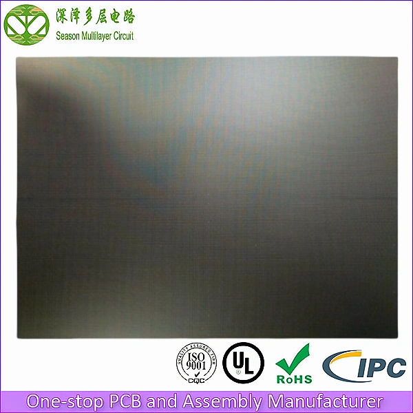
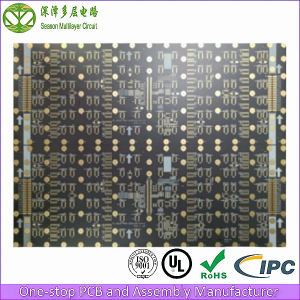
1+4+1
Layer Count
3/3 mil
Min. Trace/Space
0.10 mm
Min. Via Diameter
Tg 180
Glass Transition Temp
1–2 µ”
ENIG Gold Thickness
ISO 9001:2015
ISO 14001
UL (E305905)
IPC Class 2 / Class 3
RoHS
6-Layer HDI LED Display PCB Stackup Diagram
Our 6-layer HDI stackup for LED display applications is designed to support high-density LED matrices, high-speed video data buses, and efficient thermal dissipation in a compact, reliable package.
- Top Layer (Copper/Plated): LED pad array, driver IC placement, fine-pitch components
- Inner Layer 2 (Ground Plane): Signal reference and EMI shielding for LED driver circuits
- Inner Layer 3 (Signal Layer): High-speed video data bus routing (LVDS/MIPI)
- Inner Layer 4 (Power Plane): High-current power distribution for LED arrays and driver ICs
- Inner Layer 5 (Signal Layer): Control signal routing with buried via connections
- Bot Layer (Copper/Plated): Thermal dissipation pad and bottom-side routing
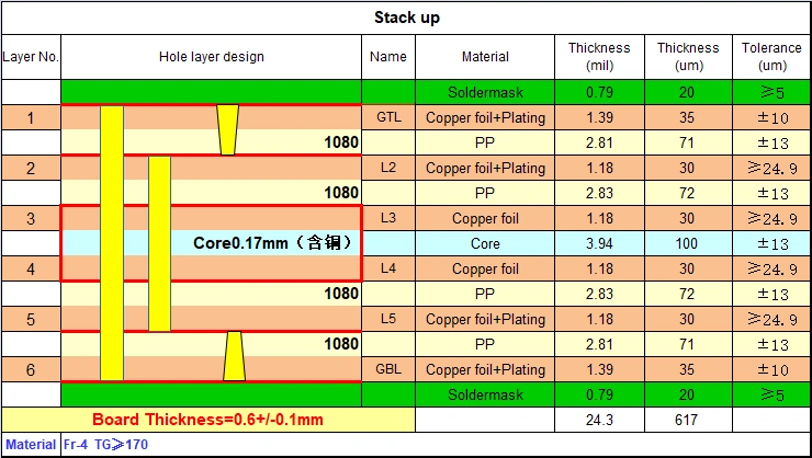
Impedance control on an LED display board applies to the high-speed video data bus, not to the LED power and driver traces. If your LVDS or MIPI interface requires a specific differential impedance, our engineering team will design an optimal stack‑up structure for your LED display layout and verify it with a Polar Instruments impedance test report on every batch.
Technical Capability & Specifications
| Parameter | Specification | Advanced Capabilities |
|---|---|---|
| Layer Count | 6-Layer HDI (1+4+1) | 2-32L(Mass); 2-64L(Sample) |
| Base Material | FR-4 S1000-2M Tg 180 | SY, NY,TUC,ZY,EMC,KB,ITEQ, Rogers, Megtron , Nelco,Isola |
| Board Thickness | 0.6mm | 0.2-6.4mm(Mass);0.15-20mm(Sample) |
| Panel Size | 400*300mm/1 | 800*600mm(Mass);1050*610(Sample) |
| Copper Thickness | Outer: 1 oz Inner: 1 oz | Outer: 1/3–12 oz Inner: 1/4–12 oz |
| Min Drill Size | 0.2mm | 0.15mm(Mass);0.127mm(Sample) |
| Min Laser Size | 0.1mm | 0.075 (Sample) |
| Min Trace Width/Spacing | 3/3mil | 2.36/2.36mil(1 oz) (Mass)2/2mil (Sample) 2/2mil(0.5 oz) 1.6/1.6mil (Sample) |
| Min BGA Pad | 0.25mm | 0.15mm |
| Surface Finish | ENIG 1–2 µ” | OSP,ENIG,HASL,Electric Hard Gold, ENIG+OSP,ENEPIG,Immersion Silver & Tin |
| Solder Mask Color | Matte Black | Green, Blue,Black,White,Yellow,Red,Purple, Matte Green,Matte Blue,Matte Black |
| Min Routing Tolerance | ±0.15mm | ±0.075mm |
| Quality Standard | IPC Class 2,RoHS | IPC Class 3, UL, RoHS,IATF 16949,GJB |
| PCB Type | HDI (1+N+1) | HDI,Multilayer,Rigid-Flex,High Frequency,High Speed,Hybrids & Mixed Dielectrics |
Key Advantages of Our LED Display PCB
- High-Current Power Distribution: 2 oz outer copper with dedicated power plane (L4) handles the high current demands of dense LED arrays without voltage drop or thermal hotspots.
- Superior Thermal Management: Optimized thermal via arrays under LED driver ICs pull heat through the board to the bottom copper layer, preventing thermal-induced color shift and extending LED lifespan.
- High-Density LED Routing: HDI blind and buried vias enable fine-pitch LED pad routing (P0.9 and below) with clean signal paths between driver ICs and LED arrays.
- Controlled Impedance Video Bus: 100 ohm differential pair routing for LVDS/MIPI video data buses ensures error-free image data transmission at high refresh rates (3840Hz+).
- Black Solder Mask Standard: Black solder mask minimizes light reflection between LEDs, improving contrast ratio and color accuracy for professional-grade displays.
Overcoming Critical Challenges in LED Display PCB Design
When sourcing HDI PCBs for LED display applications, engineers encounter three major challenges. Here is how our engineering team eliminates them:
1. Thermal Hotspots and LED Color Shift
The Problem: High-density LED arrays generate significant heat concentrated in small areas. Poor thermal management causes localized hotspots that shift LED color temperature, reduce brightness uniformity, and shorten LED lifespan.
Our Solution: Our 6-layer stackup uses a dedicated thermal management strategy: 2 oz outer copper for heat spreading, thermal via arrays under each driver IC, and an inner power plane (L4) that doubles as a thermal spreader. This reduces junction temperatures by 15-20C compared to standard boards.
2. Signal Integrity for High-Refresh Video Data
The Problem: Fine-pitch LED displays require high-bandwidth video data at 3840Hz+ refresh rates. Poor PCB design causes EMI, signal reflection, and data corruption, resulting in visible flickering, ghosting, or frozen pixels.
Our Solution: Every high-speed signal layer is paired with a solid ground reference. Differential pair routing maintains tight 100 ohm impedance control (+/-8%), ensuring clean video data transmission. Blind and buried vias minimize signal stub lengths, reducing reflection at high frequencies.
3. Miniaturization for Fine-Pitch LED Arrays
The Problem: LED pitches below 1.0mm require extremely dense routing between LED pads and driver ICs. Conventional through-hole PCBs cannot route enough traces in the available space, forcing larger board sizes or fewer LEDs per module.
Our Solution: Our HDI technology with 0.10mm laser-drilled blind vias enables P0.9 and finer LED pitch routing. Via-in-pad technology places interconnects directly under LED pads, maximizing routing density without increasing board area.
Where Our LED Display PCBs Are Used
Our 6-layer HDI LED display PCBs power a wide range of display applications:
- Fine-Pitch Indoor LED Displays: P0.9-P1.5 pixel pitch displays for broadcast studios, control rooms, and corporate lobbies requiring ultra-high resolution.
- Outdoor LED Billboards: High-brightness, weather-resistant display modules for highway billboards and building-facade installations.
- LED Video Walls: Modular display panels for concerts, sports arenas, and live event broadcasting with seamless tiling.
- Transparent LED Displays: See-through LED screens for retail windows and architectural glass installations.
- Commercial LED Screens: Digital signage displays for retail, hospitality, and transportation hubs.
SMD, COB or MIP: How the Package Choice Changes Your LED Display PCB
LED packages reach the board in three main ways, and each one changes what the PCB has to do. Choosing the package first and designing the board around it is the fastest route to a display that yields in production.
- SMD LED modules: Discrete 0404, 0606 or 1010 LEDs are reflow-soldered onto a pad array, so the PCB sets placement accuracy through pad geometry, solder-mask openings and thermal vias. Our 3/3 mil trace/space and ±0.15 mm routing tolerance keep those pad arrays consistent across a full panel.
- COB (chip-on-board): Bare LED dice are bonded directly to the board and sealed in protective resin, so there is no package to absorb mechanical stress. COB demands flatter copper, tighter pad tolerances and a matte black solder mask to keep contrast high — which is why we build P0.9-and-below routing with via-in-pad and resin-filled microvias.
- MIP (mini and micro LED in package): Individually packaged mini or micro LEDs are reflowed like SMD parts, combining very small pixel pitch with the repairability of standard reflow assembly. MIP panels sit between SMD and COB in PCB complexity and reuse the same via-in-pad stackup.
For designs that mix packages on one panel — SMD driver-side components with COB LEDs on the front, for example — send us the stackup and we will confirm pad geometry, via-in-pad and surface finish together. We build the same stackup on custom outlines for irregularly shaped LED display boards, and our P3.91 LED module PCB is a fine-pitch module built this way.
Flatness and Moisture Protection for Large-Format LED Display PCBs
A large LED display is mechanically one flat surface made from many boards. Any warp in a single board shows up as a visible seam or a brightness step in the finished wall, and outdoor cabinets add humidity to the list of failure modes. Both are decided at the PCB stage, not on site.
- Warpage control through balanced construction: Symmetric copper distribution across the stackup, matched laminate and prepreg builds, and a confirmed finished thickness keep panels flat through reflow so modules tile evenly. Copper balance is confirmed during DFM.
- Panel and thickness options for large displays: Standard boards run on 400 × 300 mm panels at 0.6 mm; mass production supports panels up to 800 × 600 mm and thicknesses from 0.2 mm to 6.4 mm, with sample runs reaching 1050 × 610 mm and 0.15-20 mm for stiff, large-format modules.
- Moisture and corrosion protection: Outdoor and rental displays cycle between humid nights and hot, powered-on days. Surface finish, solder-mask adhesion and via plugging decide how much moisture reaches fine-pitch traces and how resistant the board is to electrochemical migration, so we confirm all three against your cabinet design.
- Verification of the flatness-critical steps: Every panel passes 100% AOI and 100% electrical testing, and our HDI process capability covers laser-drilled microvias down to 0.10 mm with ±0.15 mm routing tolerance — the tolerances that decide whether a 0.9 mm pitch module tiles cleanly.
For outdoor installations, tell us the cabinet design and the expected humidity range and we will recommend the surface finish and solder mask combination before production starts.
Our Quality Guarantee for LED Display PCBs
LED display electronics operate continuously and cannot tolerate failures. We implement rigorous testing protocols on every board:
- 100% AOI Inspection: Automated Optical Inspection scans every layer for trace breaks, shorts, and alignment errors.
- 100% Electrical Testing (E-Test): Flying probe or fixture-based testing verifies continuity and isolation.
- Thermal Imaging: Available thermal imaging verification of thermal via performance under load.
- Controlled Impedance Testing: Polar Instruments impedance test report with every batch.
- Certifications: ISO 9001:2015, ISO 14001, UL (E305905), RoHS compliant. IPC Class 2 / Class 3 available.
Why Choose Season PCB for Your LED Display PCB?
With nearly 20 years of experience in PCB manufacturing, Season Multilayer Circuit has served over 8,000 global clients in LED display, consumer electronics, and telecommunications. Our three manufacturing facilities provide capacity for both rapid prototyping and high-volume production.
We understand that LED display electronics demand consistent quality and thermal reliability. That is why every 6-layer HDI LED display PCB we ship is backed by:
- Free DFM file checking before production
- 24/7 dedicated engineering support
- Guaranteed on-time delivery
- No minimum order quantity — from 1 prototype to 100,000+ units
- Engineering fee waivers on bulk production orders
Season PCB specializes in HDI LED display PCB manufacturing for fine-pitch indoor and outdoor LED display applications. Our LED display PCB products feature high-density interconnect technology, superior thermal management, and controlled impedance routing. Each LED display PCB meets IPC standards.
For your LED display PCB needs, Season PCB provides fast turnaround, competitive pricing, and ISO-certified quality. Contact us for LED display PCB manufacturing today.
Our LED display PCB boards comply with UL safety certifications and IPC manufacturing standards. Each LED display PCB undergoes thermal stress testing and signal integrity verification. The same build scales to high volumes on 998PCB Group’s 2–30 layer PCB lines at the group’s Shenzhen campus.
Frequently Asked Questions
What LED pitch sizes can your HDI PCBs support?
Our HDI PCBs with 0.10mm laser-drilled blind vias support LED pitches down to P0.7. For P0.9 and below, we recommend via-in-pad technology with resin-filled microvias. Our 3/3 mil trace/space capability provides sufficient routing density for fine-pitch LED driver interconnects.
How do you handle thermal management for high-power LED arrays?
We use a multi-layer thermal management approach: 2 oz outer copper for heat spreading, dedicated thermal via arrays under driver ICs, and an inner power plane that doubles as a thermal spreader. For extreme thermal loads, we offer metal-core PCB (MCPCB) substrates and heavy copper (up to 12 oz).
What is the lead time for HDI LED display PCB prototypes?
Standard HDI prototype lead time is 7-10 working days. Expedited 5-day service is available. Mass production typically takes 15-20 working days depending on order volume and complexity.
What materials and surface finishes are available for HDI LED display PCBs?
The standard build is a 1+4+1 HDI stackup on FR-4 S1000-2M (Tg 180), with SY, NY, TUC, ZY, EMC, KB, ITEQ, Rogers, Megtron, Nelco, and Isola laminates available on request. Board thickness is 0.6mm standard (0.2-6.4mm range) with 1 oz copper on outer and inner layers, expandable to 12 oz for high-power LED arrays. ENIG is the standard surface finish, with OSP, HASL, electric hard gold, ENIG+OSP, ENEPIG, and immersion silver & tin optional. Solder mask is matte black as standard – it reduces LED reflection and improves display contrast – with green, blue, black, white, yellow, red, purple, and matte series available.
How do you verify quality on LED display PCBs?
Every board passes 100% AOI, which scans each layer for trace breaks, shorts, and alignment errors before lamination, plus 100% electrical testing by flying probe or fixture. Thermal imaging verification of thermal via performance under load is available for high-power designs, and a Polar Instruments impedance test report accompanies every batch. We are certified to ISO 9001:2015, ISO 14001, UL (E305905), and RoHS, with IPC Class 2 and Class 3 manufacturing available.
What panel sizes and board thicknesses do you support for LED display PCBs?
Standard LED display boards are built on 400 × 300 mm panels in 0.6 mm FR-4. Mass production supports panels up to 800 × 600 mm and thicknesses from 0.2 mm to 6.4 mm, while sample and prototype runs can reach 1050 × 610 mm and 0.15-20 mm. For very large or irregularly shaped LED display boards, panelization, stiffener options and copper balance are confirmed during DFM before production starts.
Do you support both prototypes and mass production, and how fast?
Yes — there is no minimum order quantity, from a single prototype to 100,000+ units. Standard HDI prototypes take 7-10 working days, expedited service is available in 5 working days, and mass production typically runs 15-20 working days depending on volume and complexity. Published LED display PCB lead times are listed on our lead time page, and expedited handling is quoted upfront as a one-time charge before the order is placed.
Ready to start your LED Display PCB project?
Whether you need 5 pieces for prototyping or 50,000 for mass production, our engineering team is ready to support your LED display project with DFM review, thermal analysis, and fast-turn fabrication.
Tel: (+86) 18681528532 (WhatsApp)
E-mail: roc@season-pcb.com