Book Appointment Now

Advanced 12-Layer 1-Stage HDI RK3588 Core Board PCB Manufacturing
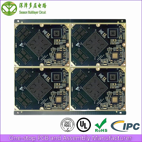
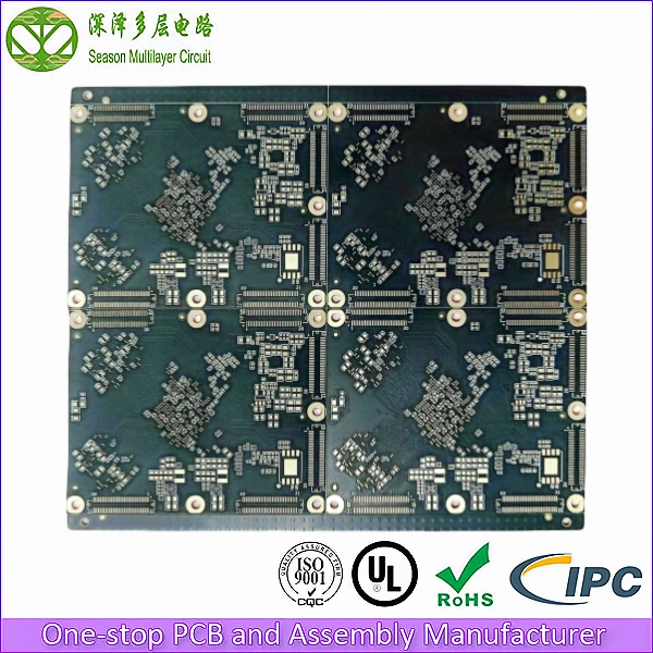
Engineered for the Rockchip RK3588 AI processor platform. Our advanced 12-layer 1-stage HDI PCB delivers exceptional signal integrity in a compact 1.2mm 1+N+1 build, supporting LPDDR5 memory, 8K video, and Gigabit Ethernet for smart TVs, projectors, industrial control, and AI edge computing.
As a specialized 12-layer HDI PCB manufacturer, Season PCB combines a proven 12-layer 1+N+1 HDI stackup, 0.10mm laser vias, 3/3mil fine-line routing, and ENIG finish with controlled impedance for HDMI 2.0, PCIe 3.0, and USB 3.0 interfaces. From 5-piece NPI prototypes to 100,000+ piece mass production, every 12-layer 1-stage HDI PCB is 100% electrically tested in our ISO 9001:2015 certified facility — with free DFM feedback within 24 hours. Explore our fast PCB manufacturing services or upload your Gerber files to get started.
Building a fine-pitch display module instead of a core board? The same 1-stage single-sequential-lamination approach drives our 4-layer 1-stage HDI irregular LED display PCB for P1.5625 creative LED screens with 0.10 mm laser microvias.
Scaling beyond a 1-stage build? Our 14-layer 2-stage HDI prototype PCB adds a second sequential microvia stage on a 2+10+2 laminated core — the same 0.10 mm laser blind vias and TDR impedance reporting, with 5-7 working day prototype lead time.
✓ 0.10mm Laser Blind Vias
1+N+1 12-layer HDI stackup
✓ 3/3mil Trace & Space
High-density fine-line routing
✓ Tg 180°C High-Tg FR-4
Dimensional stability through lead-free reflow
✓ ENIG 1–2 µ” Finish
Ultra-flat pads for fine-pitch BGA assembly
✓ 24h DFM Review
Free engineering feedback
✓ Turnkey PCBA
Component sourcing + SMT assembly
1+10+1
Layer Count
3/3mil
Min. Trace / Space
0.3mm
Min. Laser Via
Tg 180
Glass Transition Temp
1–2 µ”
ENIG Surface Finish
ISO 9001:2015
ISO 14001
UL (E305905)
IPC Class 2 / Class 3
IATF 16949
RoHS
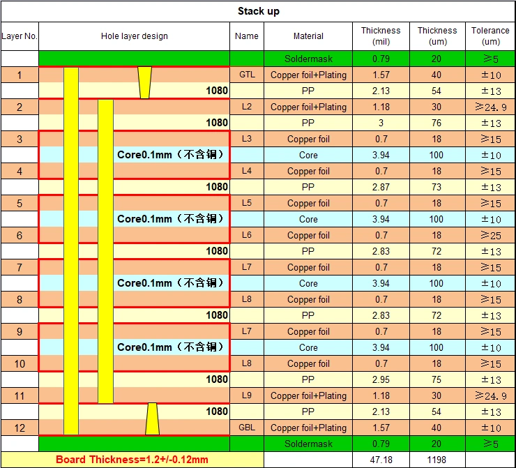
12-Layer 1-Stage HDI RK3588 Core Board PCB Stackup Diagram
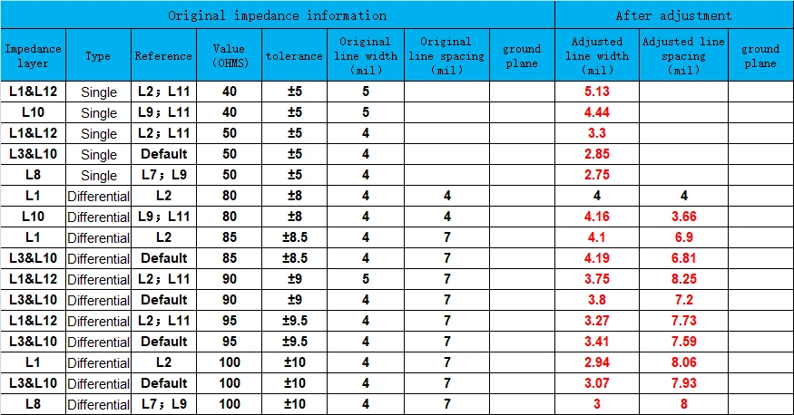
This proven 12-layer 1+N+1 HDI stackup architecture dedicates ground and power planes adjacent to each signal layer, minimizing crosstalk, ensuring clean return paths, and maintaining tight 90Ω/100Ω differential impedance control for HDMI 2.0, PCIe 3.0, USB 3.0, and MIPI CSI-2/DSI high-speed interfaces.
- L1 (Top) – Signal: Component placement and microvia layer (35μm Cu + plating).
- L2 – Ground (GND): Reference plane for L1, tied by 0.10mm laser blind vias.
- L3 – Inner Signal: High-speed routing (HDMI 2.0, PCIe 3.0, MIPI CSI-2/DSI).
- L4 – PWR Plane: Core power distribution (VDD_CPU, VDD_GPU, VDD_NPU).
- L5 – Ground (GND): Isolation & return path for L3/L4 signal layers.
- L6 – Inner Signal: LPDDR4/4X/5 memory interface routing.
- L7 – Inner Signal: Memory fan-out and control signals.
- L8 – PWR Plane: I/O and memory power rails.
- L9 – Ground (GND): Shielding for bottom-side signal routing.
- L10 – Inner Signal: Bottom-side high-speed signal routing.
- L11 – Inner Signal: Memory and I/O signal fan-out.
- L12 (Bottom) – Signal: Bottom component pads and microvia layer (35μm Cu + plating).
💡 Custom Stackup Optimization: If your existing design cannot meet stringent impedance requirements, our engineering team provides pre-production stackup optimization — adjusting dielectric thicknesses, copper weights, and material selections to hit your target impedance values. All stackups are validated using Polar CITS800s simulation before fabrication.
Technical Specifications & Manufacturing Capabilities
Every specification below reflects our proven mass-production capability, not just laboratory limits. Values marked “Sample capability” represent our advanced quick-turn prototyping tier.
| Parameter | Specification | Advanced Capabilities |
|---|---|---|
| Layer Count | 12-Layer 1-Stage HDI | 2-32L(Mass); 2-64L(Sample) HDI Any layer (Sample) |
| Base Material | FR-4 S1000-2M Tg 180 | SY, NY, TUC, ZY, EMC, KB, ITEQ, Rogers, Megtron, Nelco, Isola |
| Board Thickness | 1.2mm±0.12 | 0.2-6.4mm(Mass);0.15-20mm(Sample) |
| Panel Size | 140*120mm/4 | 800*600mm(Mass);1050*610(Sample) |
| Copper Thickness | Outer: 1 oz Inner: 0.5 oz | Outer: 1/3–12 oz Inner: 1/4–12 oz |
| Min Drill Size | 0.20mm | 0.15mm(Mass);0.127mm(Sample) |
| Min Blind Via | 0.1mm | 0.075 (Sample) |
| Min Buried Via | 0.2mm | 0.127 (Sample) |
| Min Trace Width/Spacing | 3/3mil | 1 oz: 2.36/2.36mil (Mass); 2/2mil(Sample) 0.5 oz: 2/2mil(Mass);1.8/1.8mil(sample) |
| Min BGA Pad | 0.20mm | 0.15mm |
| Surface Finish | ENIG 1–2 µ” | OSP,ENIG,HASL,Electric Hard Gold, ENIG+OSP,ENEPIG,Immersion Silver & Tin |
| Specialized Processes | POFV | Resin Plugged Vias,Copper Paste Via Filling, Copper Plating Via Filling |
| Solder Mask Color | Matte Black | Green, Blue,Black,White,Yellow,Red,Purple, Matte Green,Matte Blue,Matte Black |
| Impedance Control | ±10% (40/50/80/85/90/95/100Ω) | ±5% (Strict Tolerance) |
| Min Routing Tolerance | ±0.15mm | ±0.075mm |
| Quality Standard | IPC Class 2, RoHS | IPC Class 3, UL, RoHS, IATF 16949, GJB |
| PCB Type | HDI 1-Stage | HDI,Multilayer,Rigid-Flex,High Frequency,High Speed,Hybrids & Mixed Dielectrics |
High-Density 12-Layer 1-Stage HDI RK3588 Core Board PCB — Built for Performance, Reliability & Scale
The 12-layer 1-stage HDI RK3588 PCB from Season PCB (Season Multilayer Circuit) is a high-density interconnect (HDI) printed circuit board engineered for Rockchip RK3588 core modules. Leveraging 3/3mil trace/space precision, a 1.2mm 1+N+1 HDI build, and rigorous impedance control across 12 conductive layers, this board delivers the routing density, signal integrity, and manufacturing consistency demanded by 12-layer 1-stage HDI PCB developers and OEMs worldwide.
Designed around the Rockchip RK3588 platform — an 8-core Cortex-A76/A55 processor at 2.4 GHz with a 6 TOPS NPU — the board supports LPDDR4/4X/5 memory, 8K video decode, HDMI 2.0, MIPI-DSI, Gigabit Ethernet, USB 3.0, and PCIe 3.0. Season PCB has delivered high-layer-count HDI core boards for RK3588, RK3568, and RK3566 platforms to global customers — with yields proven in volume production.
What Makes This 12-Layer 1-Stage HDI RK3588 Core Board PCB Exceptional
1.2mm Compact 12-Layer HDI Profile
A compact 1.2mm 12-layer 1+N+1 HDI build that fits core modules for smart TVs, projectors, and industrial devices without compromising layer count or signal performance.
3/3mil Trace Space
Class-leading fine-line capability enables clean high-density BGA fan-out routing for the RK3588’s 0.20mm-pitch package with hundreds of fine-pitch balls. Achieved through LDI exposure and vacuum etching.
0.10mm Laser Blind Vias
1–2 µ ENIG on pads delivers an ultra-flat soldering surface for fine-pitch BGA assembly, with excellent oxidation resistance and consistent solder joint quality across thousands of pads.
Controlled Impedance ±10%
Strictly controlled 50Ω single-ended and 90Ω/100Ω differential impedance across all high-speed traces. Every batch undergoes TDR testing to guarantee HDMI 2.0, PCIe 3.0, and USB 3.0 signal integrity.
1+N+1 1-Stage HDI Build
Laser-drilled 0.10mm blind microvias connect L1→L2 and L12→L11, freeing inner routing channels for dense signal traces while preserving continuous ground and power planes.
High-Tg FR-4 Material (Tg 180°C)
Built with FR-4 S1000-2 Tg 180 high-Tg laminate rated at Tg 180°C, ensuring dimensional stability and delamination resistance through multiple lead-free reflow cycles with peak temperatures approaching 260°C.
100% AOI & E-Test Inspection
Every single board passes automated optical inspection (AOI) on all layers and 100% netlist electrical testing. TDR impedance verification, cross-section analysis, and IST reliability testing are performed on every lot.
Turnkey PCB + PCBA Service
One partner for the entire product lifecycle — from quick-turn HDI prototyping and volume PCB fabrication to component procurement, SMT assembly, reflow soldering, and functional testing. Reduce supply-chain complexity.
Where the RK3588 Core Board Delivers Maximum Impact
Smart TV
4K/8K streaming, voice-interactive display, multi-screen casting
4K/8K Projectors
Ultra-short-throw, laser phosphor, home theater and business projection
Intelligent Vending Machines
Smart inventory, cashless payment, facial-recognition dispensing
Security & Surveillance
Multi-channel NVR, AI face recognition, behavior analytics
Industrial Control & Automation
PLC, HMI panels, motor drives, factory automation gateways
AI Edge Computing
6 TOPS NPU inference, machine vision, predictive maintenance
Four Pillars of the RK3588 Core Board Built on Our 12-Layer HDI PCB
1. Blazing-Fast 8-Core Processing
The quad-core Cortex-A76 delivers approximately 20% higher performance than the previous-generation Cortex-A73, while the quad-core Cortex-A55 handles background tasks efficiently. Combined with LPDDR4/4X/LPDDR5 memory and eMMC 5.1 storage, the 12-layer 1-stage HDI PCB achieves extraordinary throughput for AI inference, video processing, and multitasking.
2. Exceptional Energy Efficiency
The big.LITTLE architecture cuts power consumption by roughly 20% versus Cortex-A73 at equivalent performance. An advanced Power Management Unit (PMU) and low-power I2S audio interface further extend battery life and reduce thermal output — critical for fanless smart devices operating 24/7.
3. Comprehensive I/O & Video Ecosystem
One 12-layer 1-stage HDI PCB, limitless application scenarios: HDMI 2.0, MIPI-DSI, and CVBS for multi-channel video; I2S/PCM audio with voice recognition; Gigabit Ethernet, USB 3.0/2.0, SPI, I2C, UART, and PCIe 3.0 for universal peripheral connectivity.
4. Industrial-Grade Reliability
FR-4 Tg 180 high-Tg laminate and advanced fabrication processes deliver rock-solid mechanical and electrical stability. Multiple boot options (NAND Flash, SD, eMMC) and dual-OS support (Linux and Android) ensure deployment flexibility across every project requirement.
Pushing Precision to the Limit — How We Build It
Producing this 12-layer 1-stage HDI PCB with 0.10mm laser microvias and 3/3mil trace/space is not a routine fabrication job — it demands world-class process control, specialized equipment, and deep domain expertise. Here’s how we solve the two hardest challenges.
Challenge #1: 0.10mm Laser Blind Vias in a 1+N+1 HDI Build
The Problem
The RK3588’s 0.20mm-pitch BGA packs hundreds of fine-pitch balls into a single package. Escaping every signal ball requires via-in-pad or blind-via fan-out — but traditional mechanical through-holes (0.20mm+) consume too much routing space and block inner signal paths. Only 0.10mm laser blind vias connecting L1→L2 and L12→L11 free the inner routing channels while preserving continuous ground and power planes.
Our Solution
➔ High-precision UV/CO² laser drilling creates 0.10mm blind microvias with clean, consistent sidewalls for reliable plating.
➔ VCP (Vertical Continuous Plating) ensures void-free copper metallization inside every microvia.
➔ Desmear treatment removes drilling residue, guaranteeing robust inter-layer connections.
➔ 100% AOI plus X-ray inspection verify via alignment and plating quality before shipment.
Challenge #2: 3/3mil Fine-Line Routing at 12-Layer Density
The Problem
Routing the RK3588’s HDMI 2.0, PCIe 3.0, USB 3.0, and MIPI CSI-2/DSI interfaces through a 12-layer stackup requires 3/3mil trace and space fine-line geometry — with ten inner layers imaged and etched to micron-level uniformity. Any deviation in line width causes impedance mismatch, leading to signal reflection, insertion loss, and EMI at multi-gigabit speeds. Interlayer registration across two lamination cycles must stay within ±50 µm.
Our Solution
➔ LDI direct-imaging exposure and vacuum etching deliver consistent 3/3mil fine-line quality across all ten inner layers.
➔ Two-stage lamination (10-layer core, then outer-foil bonding) with dimensional stability compensation achieves alignment within ±50 µm.
➔ Automated impedance testing verifies every board against 90Ω/100Ω differential targets.
➔ 100% flying-probe electrical testing plus AOI on every layer guarantee zero-defect delivery.
Rigorous Testing — Every Board, Every Batch
Before any RK3588 PCB leaves our facility, it passes through a multi-stage quality assurance gauntlet. We don’t sample-test — we test 100% of boards and validate every production lot.
Automated Optical Inspection
100% optical scan of inner and outer layers for open/short detection
Flying Probe / E-Test
100% netlist electrical testing for continuity and isolation verification
TDR Impedance Testing
Time-domain reflectometry on controlled-impedance traces (±10%)
Cross-Section Analysis
Microsection inspection of plated through-holes, via fill quality, and inter-layer registration. Verifies copper plating thickness uniformity and void-free resin plugging.
Thermal Stress / IST
Wetting balance and dip-and-look testing per IPC-J-STD-003. Interconnect Stress Testing validates reliability under simulated reflow thermal cycling.
X-Ray Inspection
Non-destructive BGA void analysis and internal layer alignment verification. Critical for confirming void-free via plugging and pad flatness under fine-pitch components.
Six Reasons Global Core Board Brands Choose Season Multilayer Circuit
10+ Years of Proven HDI PCB Production
Volume manufacturing of high-layer-count HDI PCBs for RK-series core boards, with continuous process refinement and yield optimization.
0.10mm Laser Via Precision at Scale
LDI exposure, vacuum etching, and AOI ensure consistent micro-scale trace quality batch after batch.
±10% Impedance Control
Tight impedance tolerance for single-ended and differential pairs, verified by TDR testing on every lot.
One-Stop PCB + PCBA Service
From HDI prototyping and volume PCB fabrication to component sourcing and SMT assembly — a single supply chain partner.
IPC Class 2 / Class 3 Compliance
Rigorous quality assurance including flying probe, AOI, X-ray, cross-section analysis, and IST reliability testing.
Global Delivery & Support
English-speaking engineering support, DHL/FedEx/UPS logistics, and flexible payment terms for international clients.
Compatible with All Major Rockchip RK-Series Platforms
Our 12-layer 1-stage HDI PCB is validated across the industry’s leading Rockchip ecosystems. Whether you’re designing around the flagship RK3588, the cost-optimized RK3568, the compact RK3566, or a fully custom SoM — our board delivers first-pass success.
RK3588 / RK3588S
Flagship 8-core Cortex-A76/A55 with 6 TOPS NPU, 8K decode, and LPDDR5 support. Optimized HDI fan-out for AI, Smart TV, and multimedia core boards.
RK3568
Quad-core Cortex-A55 with dual display outputs. Proven 12-layer HDI routing for industrial control and HMI applications.
RK3566
Cost-efficient quad-core platform for smart home hubs and IoT gateways. Compact HDI build for space-constrained devices.
Custom RK SoM
Custom stackups, impedance profiles, and panelization for your specific RK-series SoM. Engineering support from DFM review to volume production.
The Future of Core Board PCB Technology — What’s Next
▶ Advanced HDI & Anylayer Technology
As AI and 8K multimedia demand ever-higher processing density, core board PCBs are evolving toward 2-stage and Anylayer HDI architectures with stacked microvias. These technologies shorten signal paths, reduce parasitic capacitance, and unlock faster processor platforms.
▶ Ultra-Low-Loss & High-Tg Materials
An 8-core SoC drawing 10–15W under full load makes heat dissipation critical. Next-gen core board PCBs adopt embedded copper coins, thermal vias under the BGA, and high-Tg (>200°C) laminates to maintain electrical and mechanical stability under thermal stress.
▶ AI, Cloud & IoT-Driven Demand Surge
The explosive growth of edge AI inference, smart retail, and industrial IoT is driving demand for custom RK-series core board PCBs in smart TVs, vending machines, security systems, and edge AI boxes. We are scaling production to meet this multi-sector demand.
As a specialized HDI core board PCB manufacturer, Season PCB delivers high-quality 12-layer 1-stage 12-layer HDI PCB solutions for RK3588 core board applications. Our 12-layer HDI PCB manufacturing expertise covers 4-layer to 12-layer designs with precise impedance control for high-speed signal integrity.
Every RK3588 PCB we produce undergoes rigorous testing to ensure reliable performance in demanding smart device environments. Contact us for your core board PCB manufacturing needs.
Season PCB specializes in 12-layer HDI PCB manufacturing for RK3588 core board applications. Our production process ensures precise impedance control for LPDDR5, HDMI 2.0, and PCIe 3.0 signals. Every board is manufactured with high-Tg FR-4 laminate and tested to meet stringent signal integrity requirements. Contact us for your core board PCB manufacturing needs.
Our HDI core board PCB manufacturing follows Rockchip platform guidelines for RK-series reference designs and IPC manufacturing standards. Each 12-layer 1-stage HDI PCB undergoes impedance verification and thermal cycling tests. Volume programmes of this build run on 998PCB Group’s advanced HDI PCB lines under the same quality system.
Frequently Asked Questions
Common inquiries about 12-layer 1-stage HDI RK3588 PCB manufacturing
What is a 12-layer 1-stage HDI PCB for RK3588 applications?
A 12-layer 1-stage HDI PCB is a high-density interconnect circuit board with twelve copper layers, manufactured using a 1+N+1 (1+10+1) stack-up. The 1-stage designation means the board undergoes two lamination cycles: first to create a 10-layer core, then to bond two outer copper foils. Laser-drilled blind microvias (as small as 0.10mm) connect the outermost layers to their adjacent inner layers, achieving extreme routing density for high-pin-count BGA processors like the RK3588.
Why is the RK3588 processor ideal for core board designs?
The Rockchip RK3588 combines a quad-core Cortex-A76 and quad-core Cortex-A55 big.LITTLE architecture running at up to 2.4 GHz, with an integrated 6 TOPS NPU for AI inference. It supports LPDDR4/4X/5 memory, 8K video decode, multiple display outputs (HDMI 2.0, MIPI-DSI, CVBS), Gigabit Ethernet, USB 3.0, and PCIe 3.0, running both Linux and Android. This versatility makes it ideal for AI, smart TV, industrial control, and security applications — all on a single core board platform.
Why use ENIG surface finish for the RK3588 core board?
Electroless Nickel Immersion Gold (ENIG) with 1–2 µ” gold provides an ultra-flat soldering surface that is essential for the RK3588’s 0.20mm-pitch BGA package. ENIG offers excellent oxidation resistance (long shelf life), superior wire-bonding compatibility, and consistent solder joint quality across thousands of fine-pitch pads — ensuring zero-defect assembly and reliable long-term operation.
Can Season PCB provide full turnkey PCBA for the RK3588 core board?
Yes. We offer a complete one-stop PCB and PCBA solution: 12-layer HDI bare board fabrication, RK3588 BGA and memory component sourcing from authorized Rockchip distributors, fully automated SMT placement with X-ray-inspected BGA reflow, DIP through-hole assembly, conformal coating, functional testing, and OS (Linux/Android) flashing. The result is a ready-to-integrate core module delivered to your production line.
What is the typical lead time for 12-layer 1-stage HDI PCB prototyping?
For 12-layer 1-stage HDI prototypes, our standard lead time is 7–10 working days for bare boards, with expedited options (5–7 days) for urgent projects. Volume production typically runs 12–18 days depending on quantity and complexity. Contact our engineering team with your Gerber files for a project-specific quote and schedule.
Ready to Launch Your RK3588 Core Board Project?
Whether you need 5 prototype boards for design validation or 100,000 units per month for mass production — our team is ready. Send us your Gerber files and receive a detailed DFM review and quotation within 24 hours.