Skip to content
  • Home
  • Services
  • Products
    • Fast PCB
    • Multilayer PCB
    • HDI PCB
    • High Speed PCB
    • High Frequency PCB
    • Rigid-Flex PCB
    • PCBA
  • Instant PCB Quote
  • About Us
    • Company Profile
    • Factory Display
    • Process Capability
    • Lead Time
    • HDI PCB Technology
    • PCB Materials and Laminates
  • News
  • Contact

Book Appointment Now

(+86) 1868152853224/7 Emergency Phone
Season PCB logo - PCB manufacturer in Shenzhen, China
  • Home
  • Services
  • Products
    • Fast PCB
    • Multilayer PCB
    • HDI PCB
    • High Speed PCB
    • High Frequency PCB
    • Rigid-Flex PCB
    • PCBA
  • Instant PCB Quote
  • About Us
    • Company Profile
    • Factory Display
    • Process Capability
    • Lead Time
    • HDI PCB Technology
    • PCB Materials and Laminates
  • News
  • Contact
(+86) 1868152853224/7 Emergency Phone
Season PCB logo - PCB manufacturer in Shenzhen, China

Stackup & Impedance

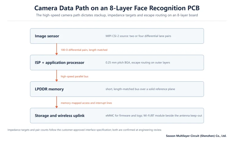
Block flow diagram of the camera data path on an 8-layer face recognition PCB, from image sensor through ISP and processor to memory and wireless uplink

8-Layer Face Recognition PCB: Stackup, Signal Path and Manufacturing

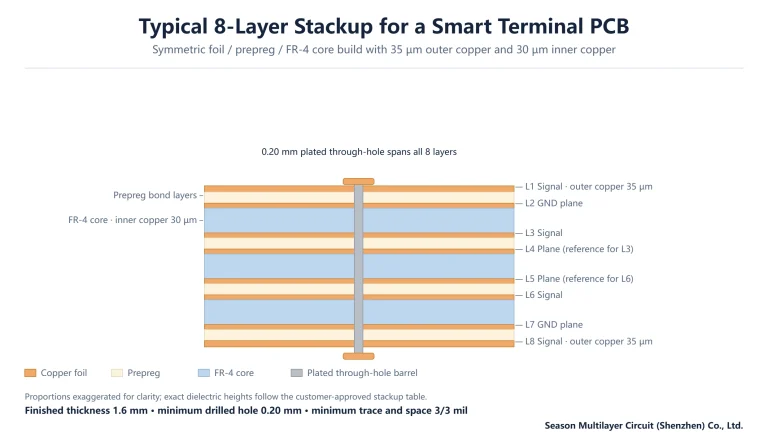
Cross-section diagram of an 8-layer smart terminal PCB stackup with copper foil, prepreg, FR-4 cores and a plated through-hole

8-Layer Smart Terminal PCB: Stackup, Design Rules and Manufacturing

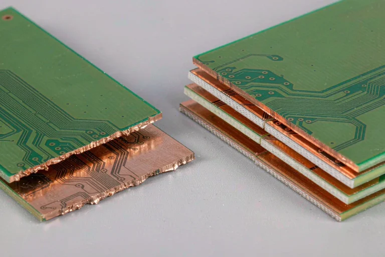
Exploded stack of a two-layer double-sided PCB next to a four-layer multilayer PCB showing the two inner copper planes and prepreg bonds

2-Layer vs 4-Layer PCB: Structure, Performance and Cost Compared

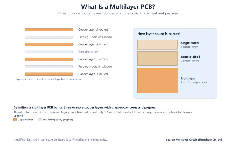
Exploded diagram of a multilayer PCB showing four copper layers separated by insulating cores and prepreg, with a layer-count ladder from single-sided to multilayer

What Is a Multilayer PCB? Layers, Stackup and Uses Explained

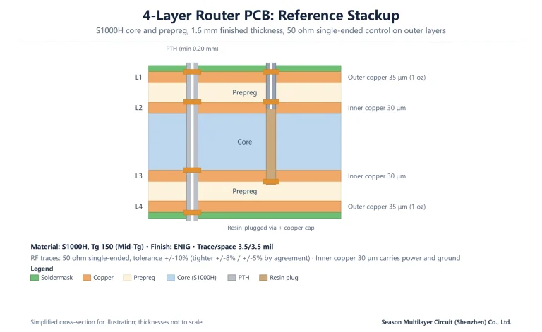
Reference 4-layer router PCB stackup on S1000H Tg 150 material with 50 ohm controlled impedance outer layers

4-Layer Router PCB: Stackup, RF Layout and Material Choice

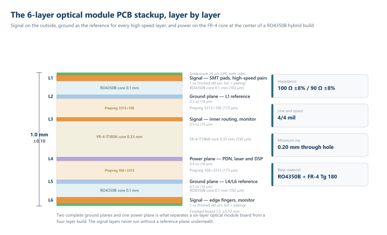
6-layer optical module PCB hybrid stackup cross section: L1 signal pairs on RO4350B, L2 ground, L3 inner routing on FR-4 IT180A, L4 power, L5 ground and L6 gold fingers, 1.0 mm finished thickness

6-Layer Optical Module PCB: Stackup, Impedance and Finish

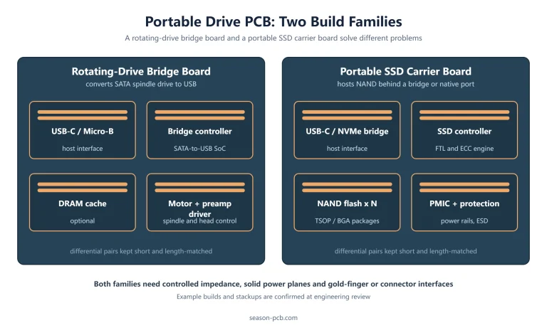
Diagram comparing a rotating-drive bridge board and a portable SSD PCB carrier board with their typical components and signal classes

Portable SSD PCB: Proven 10-Layer Stackup and Gold Finger Rules

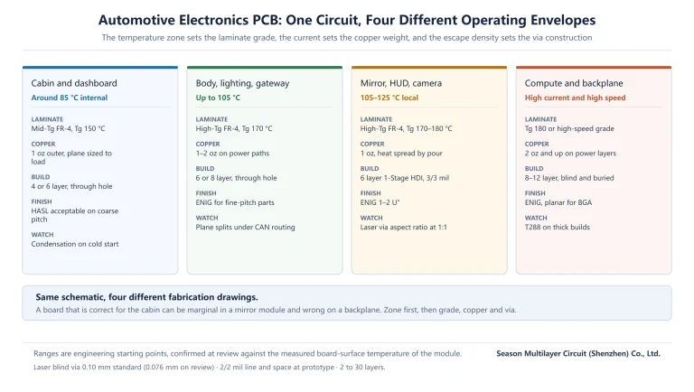
Four automotive electronics PCB operating envelopes showing how the temperature zone sets the laminate grade, copper weight and via construction

Automotive Electronics PCB: Materials, Stackup and Process Rules

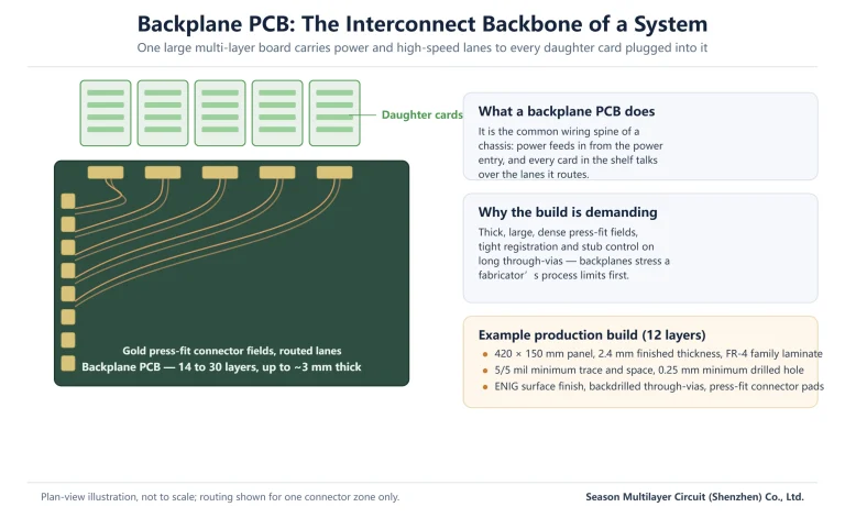
Plan view of a backplane PCB with press-fit connector zones, routed differential pairs and daughter cards plugged into the top edge

Backplane PCB Design: Stackup, Connectors and Stub Control

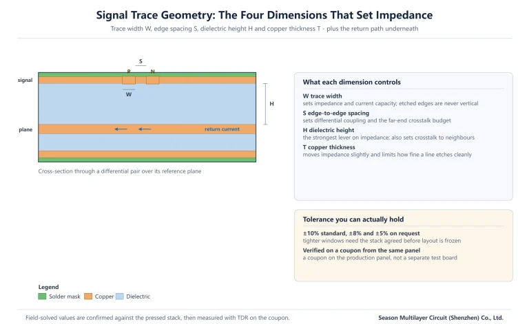
Signal trace cross-section showing trace width, edge spacing, dielectric height, copper thickness and the return current path over a reference plane

PCB Signal Trace Design: Routing Rules That Hold Up in Production

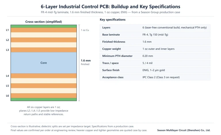
6-layer industrial control PCB buildup with 1.6 mm thickness, 1 oz copper, FR-4 Tg 150 laminate and ENIG finish

6-Layer Industrial Control PCB: Best Specs, Stackup and Sourcing

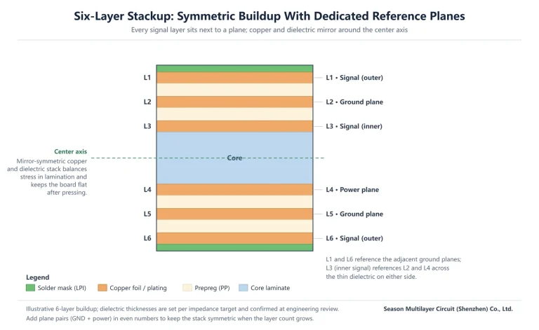
PCB stackup design example: six-layer cross-section with ground and power reference planes and a mirror-symmetric buildup

PCB Stackup Design: 8 Rules for Signal Integrity and Cost

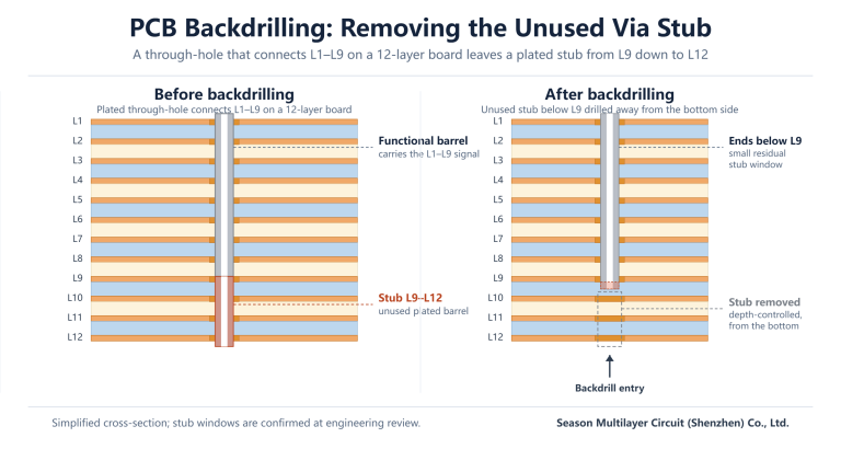
PCB Backdrilling Explained: Via Stub Removal for Signal Integrity

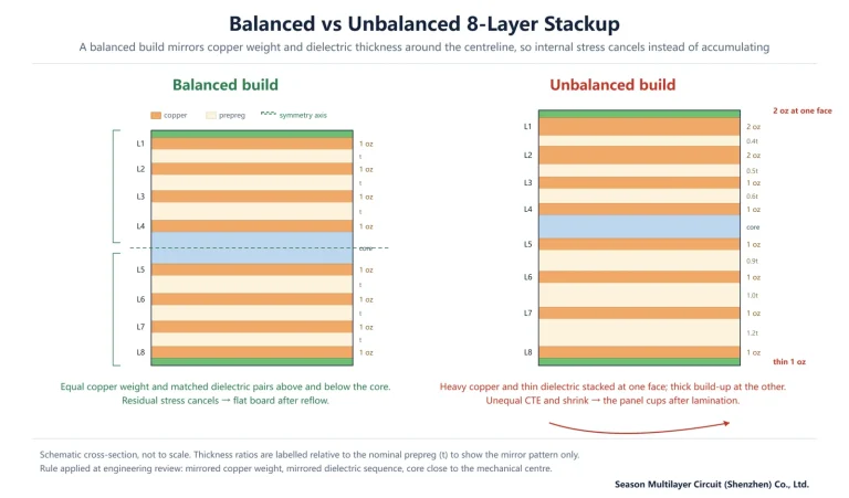
Balanced versus unbalanced 8-layer PCB stackup with mirrored copper weight and dielectric thickness around the symmetry axis

Balanced PCB Stackup Design: Symmetry, Copper Balance and Warpage Control

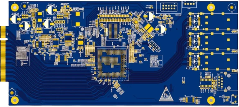
Four-layer high-speed PCB with controlled-impedance routing and a gold edge connector, 1097x491

What Is a High-Speed PCB? Design Rules, Stackup and Manufacturing Limits

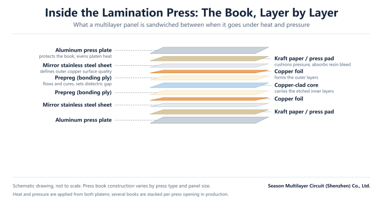
PCB Lamination Process: How Multilayer Boards Are Pressed and Bonded

How to Choose a Multilayer PCB Manufacturer: A 5-Step Checklist

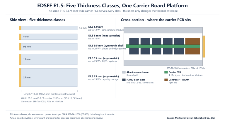
E1.S SSD PCB Design: EDSFF Carrier Board Stackup and Fabrication Rules

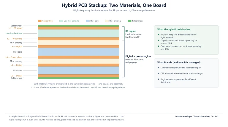
Cross section of a 6-layer hybrid PCB stackup with the RF signal and ground pair on a low-loss laminate above FR-4 cores carrying the digital and power layers

Hybrid PCB Stackup Guide: Mixed Dielectric Materials, Cost and Uses

Layered PCB laminate construction showing copper foil, prepreg and core materials

PCB Laminate Selection Guide: From Standard FR4 to Low-Loss Materials

1 2
Next
About Us
We are a professional manufacturer specialized in HDI and multilayer PCBs, focusing on advanced manufacturing processes for high-end HDI, multilayer PCBs, flexible printed circuits (FPCs), and rigid-flex boards, along with comprehensive services including SMT processing and PCBA OEM/ODM solutions with material procurement.
Main Products
HDI PCB
Fast PCB Sample
Multilayer PCB
High Frequency PCB
High Speed PCB
Rigid-Flex PCB
PCBA turnkey service
Resources
PCB Basics
HDI & Microvias
Stackup & Impedance
Materials & Surface Finishes
Manufacturing Process
Assembly & Test
Standards & Certification
Industry News
Address
7F, Block A, Junfeng Business Building, 176 Chongqing Road, Fuhai Street, Baoan District, Shenzhen 518103
Tel: +86 18681528532
E-mail: roc@season-pcb.com

Copyright © 2006-2026 Season Multilayer Circuit (Shenzhen) Co., Ltd.