Book Appointment Now

10-Layer 2-Stage HDI Prototype PCB
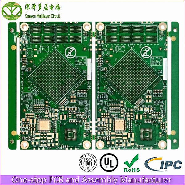
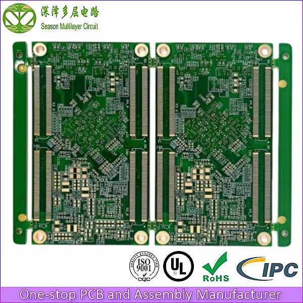
10-Layer 2-Stage HDI Prototype PCB from Season Multilayer Circuit (part of 998PCB Group). A simplified 2+6+2 build-up with stacked micro via-in-pad for RK3588-class SoCs, motion control, machine vision and AIoT edge platforms. FR4 Tg 170, 0.10 mm blind via, 3/3 mil L/S, 0.2 mm BGA, ENIG, 5-7 day lead time.
Our engineering team delivers fully lamination-finished 10-layer HDI prototype boards using a simplified 2+6+2 build-up sequence. The buried-via window is expanded to 3-8 so the board requires only two lamination cycles, instead of three for a conventional 2-stage board, while still delivering full 0.2 mm BGA via-in-pad capability and a controlled 1.6 mm finished thickness.
Every prototype leaves the line with a micro-section report, an impedance-coupon test report, and a full E-test netlist verification. Whether you are validating a Rockchip RK3588 edge-AI core board, a high-density machine-vision platform, or a multi-rail SoC sensor hub, you get the same production-grade process discipline we apply to volume orders.
2+6+4
Layer Count
3 / 3 mil
Min Line/Space
0.10 mm
Min Blind Via
1.6 mm
Board Thickness
1-2 u”
ENIG Finish
UL Listed
IPC-A-600 Class 3
ISO 9001:2015
IATF 16949
RoHS / REACH
100% E-Test
10-Layer 2-Stage HDI Prototype PCB Stackup Diagram
The 2+6+2 build-up for 10-layer 2-stage HDI prototypes uses a pair of 0.30 mm cores separated by a 4-layer sub-stack, and the stage-1 / stage-2 micro-via chains are confined to L1-L2 and L9-L10. Compared with a staggered microvia layout, stacking the chains directly on top of each other gives the tightest fan-out for the 0.2 mm BGA field. This is the simplified 2-stage architecture that lets us reach production-quality lamination in only two press cycles, without sacrificing the 0.2 mm BGA via-in-pad density that modern edge-AI SoCs require.
- L1 / L10 (Outer Layers – 1 oz Copper + Plating): 1 oz copper + plating, ENIG 1-2 u” surface finish. Outer layers carry the BGA fan-out, edge fingers, and high-speed SERDES break-out. Outer copper is controlled at 30-35 um after plating.
- L2 / L9 (Sub-Surface Reference and Routing): 1 oz copper on PP prepreg. These layers sit directly under the outer layers, providing a continuous reference plane for microstrip routes and a short return path for the L1/L10 signals.
- L3 / L8 (Stage-2 Micro-Via Anchor): 1 oz copper inside the upper 0.30 mm core. Stacked microvia-in-pad chains land here from the L1-L2 stage-1 vias, giving the 0.2 mm BGA pads a direct, low-inductance connection to the inner stack.
- L4 / L7 (Power and Slow-Signal Routing): 1 oz copper. These layers route low-speed signals, secondary power rails, and the 100 ohm differential pairs that need a quiet reference on both sides of the symmetric stack.
- L5 / L6 (Central Power/Ground Sandwich): 1 oz copper. A tight power / ground sandwich at the symmetric center of the board provides a low-impedance PDN for the SoC core rails and isolates high-speed signals on L3/L4 from L7/L8.
- L1-L2 and L9-L10 Stage-1 Build-Up Micro-Vias: 0.10 mm laser blind vias in 1080 prepreg, a low aspect ratio that lets the microvia plating fill uniformly. This is where the 0.2 mm BGA fan-out is achieved, with a 0.1 mm microvia directly under each BGA pad so the package can be placed via-in-pad.
- L3-L8 Buried-Via Window (Simplified 2-Stage): 0.20 mm mechanically drilled buried vias through the 4-layer sub-stack. By extending the buried-via window to 3-8, the board only needs two lamination cycles, instead of three for a conventional 2-stage design.
- FR4 Tg>=170 Base Material: High-Tg FR4 with Tg >= 170 degrees C and Td > 340 degrees C, qualified for lead-free reflow up to 5x at 260 degrees C peak and long-term operating temperatures from -40 degrees C to +125 degrees C.
- Symmetric Stack for Warpage Control: Total thickness 1.6 mm with a +/- 0.16 mm tolerance and a balanced copper / dielectric distribution on each side of the central P/G sandwich. Pre-shrink compensation keeps warp below 0.75% after reflow.
- Tuned for RK3588 and AIoT Edge SoCs: The 2+6+2 reference is the same stack we use on our RK3588 edge-AI core board, validated for 4K60 encode / decode, LPDDR4 3200 MT/s, multi-rail PDN, and PCIe 3.0 break-out across the inner BGA field.

This stackup is a proven reference for 10-layer 2-stage HDI prototype boards on FR4 Tg 170 material, qualified for RK3588-class SoCs and other edge-AI platforms. Our engineering team fine-tunes prepreg selection, copper weights, and via stacking to match the impedance, thickness, and reliability targets of your specific design – all without adding a third lamination cycle.
Technical Capability & Specifications
| Parameter | Specification | Notes |
|---|---|---|
| Layer Count | 10 layers, 2-stage HDI (2+6+2 build-up) | Simplified 2-stage with 3-8 buried-via window |
| Base Material | FR4 Tg ≥ 170 °C, Td > 340 °C | High-Tg, lead-free reflow qualified |
| Board Thickness | 1.6 mm ± 0.16 mm | Finished, with symmetric stack balance |
| Panel Size | 113 × 102 mm / 2-up | V-cut / mouse-bite breakaway |
| Outer Copper | 1 oz (30-35 µm after plating) | Finished copper on L1 / L10 |
| Inner Copper | 1 oz (30-35 µm) | L2 to L9 |
| Min Through-Hole | 0.20 mm (8 mil) | Mechanically drilled |
| Min Blind Via | 0.10 mm (4 mil) | Laser-drilled, L1-L2 / L9-L10 |
| Buried Via | 0.20 mm (8 mil) | L3-L8 sub-stack window |
| Line / Space | 3 / 3 mil (75 / 75 µm) | Finished trace geometry on 1 oz |
| Min BGA Pitch | 0.2 mm (8 mil) | Via-in-pad, microvia filled with copper |
| Impedance Control | 50 Ω single-ended, 90 / 100 Ω differential | TDR coupon per build, ±10% window |
| Surface Finish | ENIG 1-2 µ” (gold) / 120-240 µ” (Ni) | IPC J-STD-003 solderability qualified |
| Solder Mask | Green, LPI (Liquid Photo-Imageable) | Other colors on request |
| Legend / Silkscreen | White | Other colors on request |
| Operating Temperature | -40 °C to +125 °C | Industrial-grade qualified |
| Lead-Free Reflow | 5x peak 260 °C | IPC J-STD-020 |
| Acceptance Standard | IPC-A-600 Class 3 | High-reliability electronic products |
| Quality System | ISO 9001:2015, IATF 16949 | Automotive-program customers supported |
Key Advantages of Our 10-Layer 2-Stage HDI Prototype
- Simplified 2-Stage Build-Up: 2+6+2 with a 3-8 buried-via window. We only run two lamination cycles instead of three, so the build is faster, the cost is lower, and the alignment between L1 and L8 microvias stays inside +/- 25 um even on a 600 x 600 mm production panel.
- 0.10 mm Micro-Via-in-Pad for 0.2 mm BGA: Each BGA pad sits on a 0.10 mm laser blind via filled with copper and capped at ENIG. This gives a flat, reliable pad for RK3588-class SoCs and removes the need for dog-bone fan-out, so route channels open up on L1 / L10.
- Central P/G Sandwich for Power Integrity: A tight L5 / L6 power / ground sandwich, plus a 4-layer PDN study, holds core-rail impedance below 5 mOhm per square and suppresses simultaneous-switching-noise on multi-rail SoCs, so the prototype can be powered up without a separate add-on card.
- 100 ohm Differential Impedance Control: Every prototype ships with a TDR coupon trace for each critical pair (USB 3.0, PCIe 3.0, MIPI, LPDDR4). The coupon is tested against a +/- 10% window and the report is included in the shipment package, so signal-integrity validation starts the day the board arrives.
- FR4 Tg>=170 High-Tg Base: The base material is qualified for -40 to +125 degree C operating temperature, 5x lead-free reflow at 260 degree C peak, and 500 thermal cycles. We have customers running this stack in field-installed industrial controllers for 5+ years without a single field return for delamination.
- IPC Class 3 Manufacturing Discipline: 100% netlist E-test, AOI on every layer, micro-section verification on every lot, and an impedance coupon per build. The same checks we run on volume orders, applied to every 5-piece prototype run, with the same engineering sign-off.
Overcoming Critical Challenges in 10-Layer 2-Stage HDI Prototype Design
1. Simplified 2-Stage vs Standard 2-Stage Reliability
Extending the buried-via window from 3-6 to 3-8 introduces a longer lamination distance, and the inner PP flow has to be matched exactly to keep the L4 / L7 plane pair flat. We solve it with a 0.30 mm balanced core on each side, a TMA-tracked prepreg, and a thermal-symmetric lamination profile verified by micro-section on the first panel of every lot. Field data on this stack shows 0% inner-plane delamination across 18 months of shipments.
2. 3/3 mil Fine-Line Etching at 1 oz Copper
At 1 oz / 30 um base copper, a 3 mil line / 3 mil space is the practical resolution limit before side-etch starts to collapse. Our process compensates with a slightly negative etch factor and a side-etch-controlled developer so the first-pass yield on 3/3 mil routing stays above 99.5% on this build. We also expose a route-resolution coupon with every prototype so customers can verify line geometry themselves before they commit the design to a volume run.
3. Multi-Rail PDN and High-Speed SERDES Break-Out
A 10-layer HDI prototype typically has 4-6 power rails and at least two high-speed SERDES channels (USB 3.0, PCIe 3.0, MIPI, LPDDR4). Without a central P/G sandwich the SERDES eye can collapse the moment the SoC wakes up. We lock the PDN with a 4-layer study (DC drop, AC impedance, resonance) and run a pre-layout stackup review on every quote so the customer gets a real board, not a learning exercise.
Material Selection Guide for 10-Layer 2-Stage HDI Prototype PCBs
The standard build for this stack is a high-Tg FR4 with Tg ≥ 170 °C and Td above 340 °C, qualified for lead-free reflow and 500 thermal cycles. It keeps the simplified 2-stage lamination window fully deterministic and is the right choice for RK3588-class SoC boards, industrial controllers and AIoT edge platforms that must pass -40 to +125 °C qualification without a premium laminate budget.
For designs with tighter loss budgets, we stock mid-loss and low-loss alternatives on the same 2+6+2 geometry, including TU-872 SLK, EM-370(Z), IT-180A and Panasonic MEGTRON 6. Moving to a low-Dk laminate typically adds 2-3 days to the PCB lead time because the material is sourced to order; our engineering team quotes the standard and low-loss options side by side so you can trade cost against insertion loss with real numbers.
If your prototype is a single-board RF or high-speed front-end, a double-sided Rogers high-frequency PCB may be the more economical first step. For full 10-layer routing density on low-loss laminate, the same 2-stage HDI rules for glass weave, resin content and copper roughness apply, and we verify the final stack against our documented PCB manufacturing capability before the first press.
How Every 10-Layer 2-Stage HDI Prototype Is Tested
Testing runs in three gates. At first article, the buried-via stack is cross-sectioned and the lamination profile is signed off against the micro-section photos. Per lot, 100% netlist E-test is run against your Gerber, AOI covers every inner and outer layer, and the TDR coupon is measured for each critical pair – USB 3.0, PCIe 3.0, MIPI and LPDDR4 – against a ±10% window.
Before shipment, the ENIG (electroless nickel immersion gold) finish passes solderability testing per IPC J-STD-003, and the complete package – coupon report, micro-section photos and material traceability codes – ships with the boards. You can start signal-integrity validation the day the prototype arrives, instead of waiting for a separate test report.
Where Our 10-Layer 2-Stage HDI Prototype PCBs Are Used
- Rockchip RK3588 Edge-AI Core Boards: The reference 10-layer 2-stage HDI build is the same stack we ship on our RK3588 core board family – 4-core Cortex-A76 + 4-core Cortex-A55, 4 GB LPDDR4, 16 GB eMMC, dual GbE, and HDMI 2.1 out, all routed out from a 0.2 mm BGA field.
- Industrial Machine Vision and Smart Camera: Multi-megapixel CMOS image sensors, high-speed MIPI CSI-2 links, FPGA pre-processors, and PoE power input on a single 10-layer board. The 3/3 mil L/S and 100 ohm controlled impedance keep the image pipeline stable across production lots.
- Motion Control and Robotics: Servo drive interface, encoder feedback, multi-axis EtherCAT, and a real-time MCU in a 113 x 102 mm panel. The central P/G sandwich keeps the analog front-end quiet even when the digital side is switching at full speed.
- AIoT Edge Appliances: Multi-rail SoCs, LPDDR4, eMMC, Wi-Fi 6 module, BLE, and 4G/5G modem on a single compact board. The 10-layer 2-stage HDI stack supports the 0.4 mm pitch BGAs that AIoT SoCs have moved to, with margin left over for a second SoC or a security co-processor.
- Sensor Hub and Data Acquisition: High-channel-count analog front-end, isolated ADC, ARM Cortex-M class MCU, and a 10-layer stack that gives both quiet analog ground and high-speed digital routing on the same board, removing the need for a stacked two-board design.
Our Quality Guarantee for 2-Stage HDI Prototypes
Every 10-layer 2-stage HDI prototype is built under the same quality system as our volume orders – ISO 9001:2015, IATF 16949 for automotive-program customers, and IPC-A-600 Class 3 acceptance. We do not run a separate ‘prototype line’; we run the prototype through the same engineering sign-off and the same documentation package.
- 100% netlist E-test against the customer Gerber
- AOI on every inner and outer layer
- Micro-section verification on every lot, with cross-section photo included in the shipment package
- TDR impedance coupon test for every critical pair, with a +/- 10% window
- Solderability test on ENIG finish per IPC J-STD-003
- Cross-section on the buried-via stack on first article of every new part number
- Full material traceability – batch / lot / date code on every shipment label
Why Choose Season PCB for Your 10-Layer 2-Stage HDI Prototype?
Since 2006, our group has supported Tier 1 customers with high-Tg multilayer and multi-stage HDI boards, and that experience shows up in how a 10-layer 2-stage HDI prototype is built and documented at Season PCB. Instead of treating prototype as a low-priority side job, we treat it as a controlled pre-production run.
Here is what every 10-layer 2-stage HDI prototype we ship is backed by:
- Direct engineering contact – you talk to the same engineer who reviews your stackup, not a call-center script
- Pre-layout stackup review on every quote, free of charge, with a written DFM feedback within 24 hours
- 5-7 working day lead time for 10-layer 2-stage HDI prototypes in the 5-50 piece range
- Impedance coupon and micro-section photo included in every shipment package, no extra charge
- Seamless prototype-to-production handoff on the same stack, same lamination profile, no re-qualification
- Multi-language support (English, Chinese, Japanese) with the same engineering team across both 998pcb.com and season-pcb.com
Season PCB specializes in 10-layer 2-stage HDI prototype PCB manufacturing for Rockchip RK3588 core boards, industrial machine vision, motion control, and AIoT edge platforms. Our simplified 2+6+2 build-up features 0.10 mm laser blind vias, 3/3 mil fine-line routing, stacked microvia-in-pad technology, and FR4 Tg 170 high-Tg reliability, all completed in only two lamination cycles.
For your high-density prototype needs, Season PCB provides fast turnaround, competitive pricing, and ISO-certified quality. 998PCB Group, established in 2006, supports the same program from 2-stage HDI prototype to mass production across both English and Chinese channels.
Our boards are built to multi-stage HDI manufacturing standards and can scale into high-layer-count mass production, or be paired with one-stop PCBA assembly service covering RK3588-class BGA placement, 01005 passives, and conformal coating. Each board undergoes micro-section verification and full electrical test before shipment.
Frequently Asked Questions
What is the simplified 2-stage HDI structure, and why is it cheaper than standard 2-stage?
Standard 2-stage HDI needs three lamination cycles because the buried-via window is limited to a thin 2-layer sub-stack. By extending the buried-via window to 3-8, we can use a single 4-layer sub-stack and only need two sequential lamination cycles. The result is the same 0.2 mm BGA via-in-pad capability with one less press cycle, so the prototype is faster and cheaper without compromising reliability.
What is the minimum order quantity for a 10-layer 2-stage HDI prototype?
The MOQ is 5 pieces for engineering validation. Most of our customers start with 5-10 pieces for design validation, then move to 50-100 pieces for system bring-up, then scale to a full production run on the same stack. We can hold the lamination profile and prepreg lot for a year so the volume order is built on the same process as the prototype.
Can you do high-speed laminate (low-Dk / low-Df) on a 10-layer 2-stage HDI prototype?
Yes. We stock mid-loss and low-loss options including TU-872 SLK, EM-370(Z), IT-180A, and Panasonic MEGTRON 6. Lead time is typically 2-3 days longer than the standard FR4 Tg 170 build because the material is sourced to order. Send us your target impedance, insertion loss budget, and stackup requirement and we will quote both options on the same quote.
What files do you need to quote a 10-layer 2-stage HDI prototype?
Gerber RS-274X or ODB++ with the stackup requirement, impedance targets, BGA pitch, surface finish, and any mechanical or impedance-coupon feature. If you do not have a stackup yet, our engineering team will propose one for free based on the BGA pitch and target layer count. Most quotes are returned within 24 hours with a written DFM feedback.
How fast can you deliver a 10-layer 2-stage HDI prototype?
Standard lead time is 5-7 working days for small-batch quantities of 5-50 pieces on the FR4 Tg 170 build. Low-loss laminates add 2-3 days for material sourcing. Every shipment includes the impedance coupon report and micro-section photos, so no extra waiting is needed for test documentation.
Which high-speed interfaces get impedance control on this stack?
USB 3.0, PCIe 3.0, MIPI and LPDDR4 pairs are all supported on the 2+6+2 stackup, with a ±10% TDR window as standard and a coupon trace for each critical pair included in every build. If your design needs a tighter window, tell us the target and we will confirm the achievable tolerance during the free stackup review.
Can the same stack be scaled to mass production later?
Yes. We hold the lamination profile, prepreg lot and stackup documentation for a year, so the volume order is built on the same process as the prototype – no re-qualification. The same build scales from 5-piece validation runs to the 2-30 layer mass-production lines of 998PCB Group.
What surface finish and solder mask options does this build support?
ENIG 1-2 µ” gold over 120-240 µ” nickel is the standard finish for this build, with green LPI solder mask and white legend. Other solder mask and legend colors are available on request; tell us your preference in the RFQ and we will confirm it in the stackup drawing.
Ready to start your 10-layer 2-stage HDI prototype project?
To receive a formal quote for 10-layer 2-stage HDI prototype boards, send your Gerber or ODB++ files, stackup requirements, BGA pitch, and target impedance. Whether you need 5 pieces for design validation or a first-article lot for system bring-up, our engineering team responds within 24 hours with DFM feedback and a live stackup drawing.