Skip to content
Home
Services
Products
Fast PCB
Multilayer PCB
HDI PCB
High Speed PCB
High Frequency PCB
Rigid-Flex PCB
PCBA
Instant PCB Quote
About Us
Company Profile
Factory Display
Process Capability
Lead Time
HDI PCB Technology
PCB Materials and Laminates
News
Contact
Book Appointment Now
(+86) 18681528532
24/7 Emergency Phone
Home
Services
Products
Fast PCB
Multilayer PCB
HDI PCB
High Speed PCB
High Frequency PCB
Rigid-Flex PCB
PCBA
Instant PCB Quote
About Us
Company Profile
Factory Display
Process Capability
Lead Time
HDI PCB Technology
PCB Materials and Laminates
News
Contact
(+86) 18681528532
24/7 Emergency Phone
Menu
Manufacturing Process
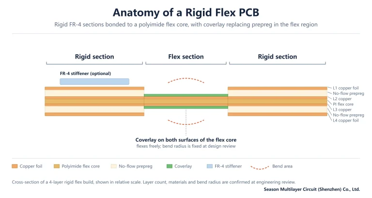
Rigid Flex PCB Explained: Structure, Manufacturing and Applications
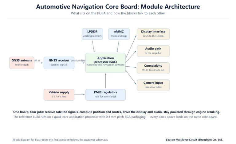
Automotive Navigation PCBA: Core Board Design and Manufacturing
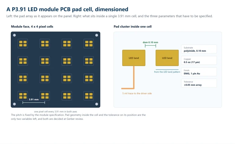
P3.91 LED Module PCB Pad Design: Geometry, Current and Finish
PCB Prototype Requirements: Parameters to Confirm Before You Order
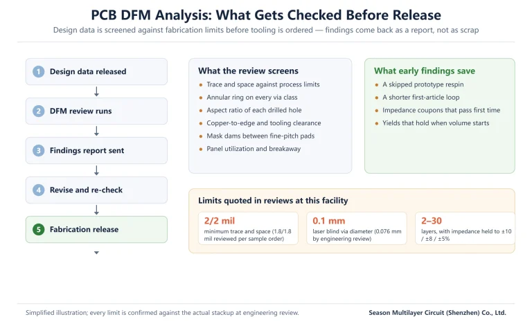
PCB DFM Analysis: What Gets Checked Before Your Gerbers Release
What Is a PCB Circuit Board? Types, How It’s Made, Where It’s Used
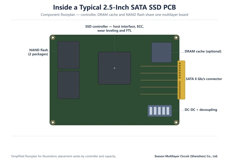
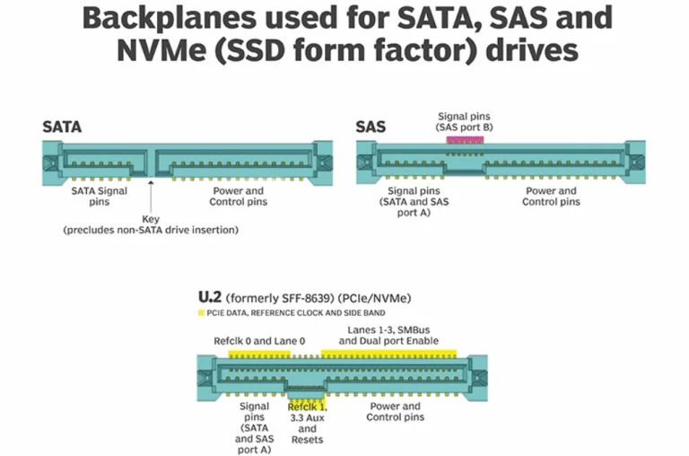
SSD PCB Design Explained: Layout, Layers and Signal Rules
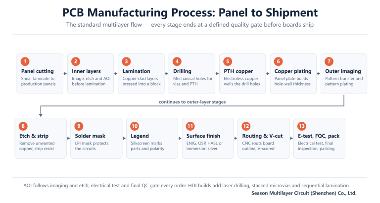
PCB Manufacturing Process: From Panel Cutting to Final Shipment
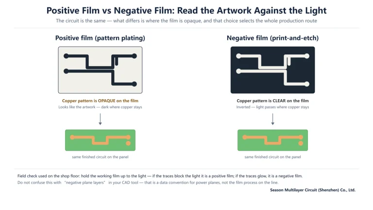
Positive Film vs Negative Film PCB: Pattern Plating and Print-and-Etch
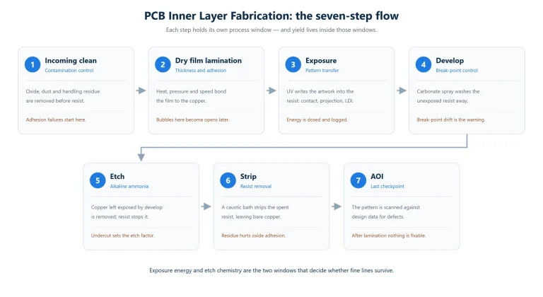
PCB Inner Layer Fabrication: Dry Film, Etching and AOI
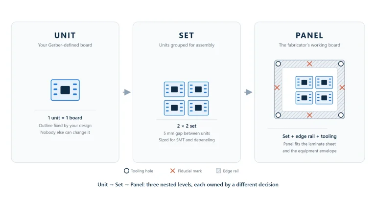
PCB Panel Cutting Explained: Unit, Set and Panel Sizing Basics
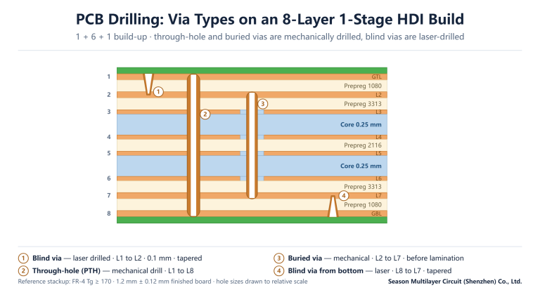
PCB Drilling Process: Mechanical vs Laser Drilling Explained
U.2 SSD PCB Design: SFF-8639 Carrier Board Layout and Build Rules
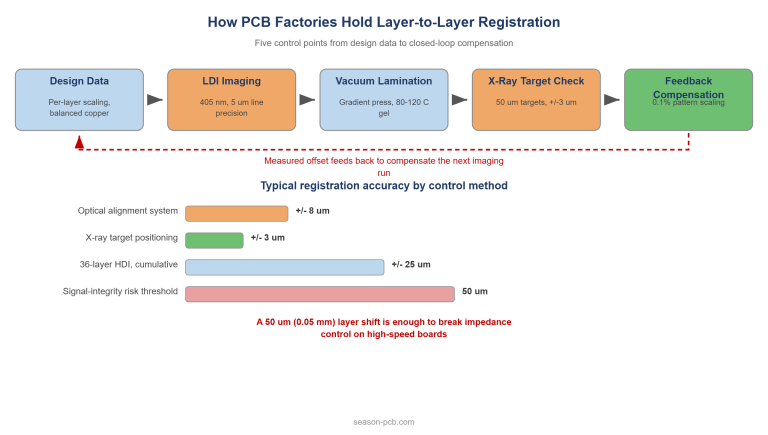
PCB Layer-to-Layer Registration Tolerance: How Factories Hold ±25 µm
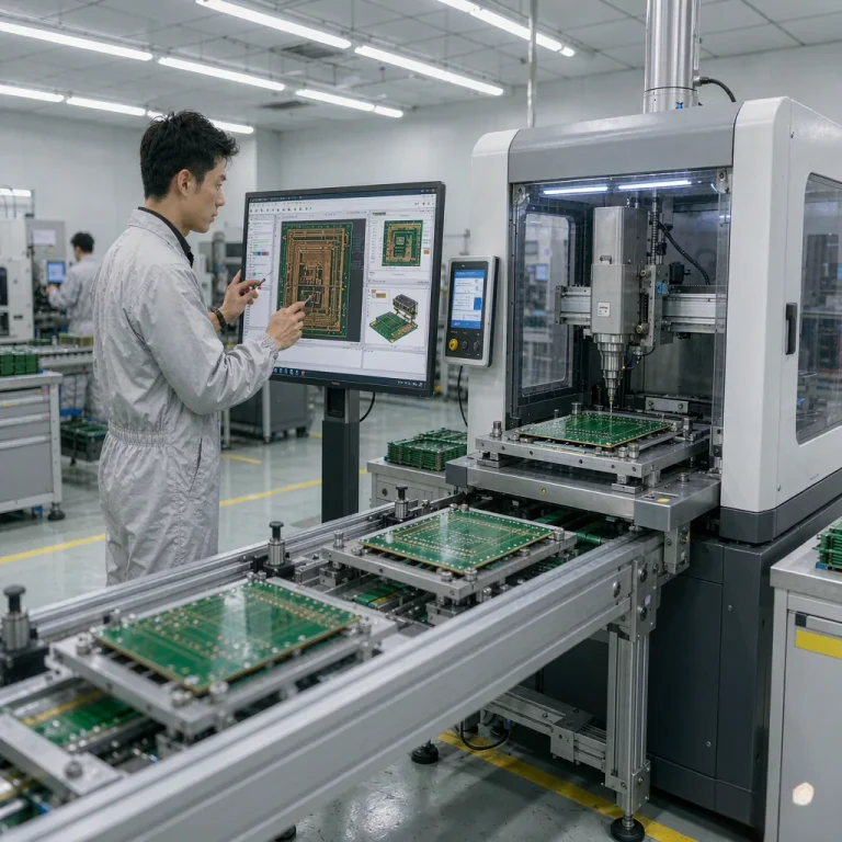
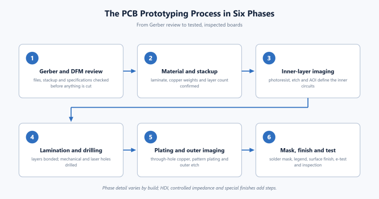
PCB Prototyping Process: From Gerber Files to First Article
PCB Reverse Engineering for Legacy Boards: Process and Limits
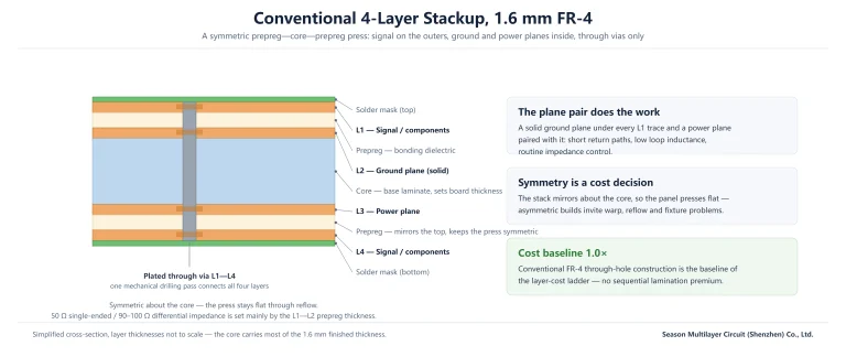
4-Layer PCB Cost: What Drives the Price and How to Quote It Right
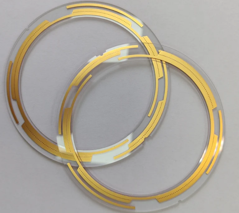
Glass Substrate PCB Explained: Properties, TGV and Where It Fits
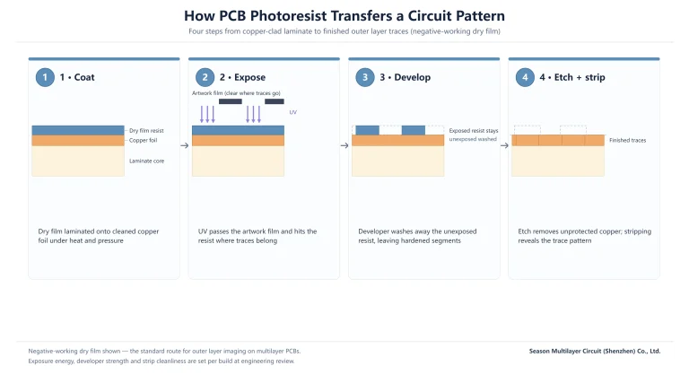
PCB Photoresist Explained: How Circuit Imaging Actually Works
Components of PCB Prices: A Practical Cost Guide for Engineers and Buyers
1
2
Next