Book Appointment Now

A 2+8+2 HDI build with 0.10 mm laser microvias and 0.2 mm BGA via-in-pad on FR-4 Tg 170, for cockpit domain controllers and ADAS sensor-fusion modules.
12-Layer 2-Stage HDI PCB for Automotive Cockpit Controllers
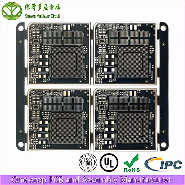
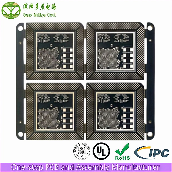
12-Layer 2-Stage HDI PCB from Season Multilayer Circuit (part of 998PCB Group). A 2+8+2 build-up – an eight-layer buried-via core with two laser microvia stages on each side – for automotive cockpit domain controllers, instrument clusters and ADAS sensor-fusion boards. FR-4 Tg 170, 0.10 mm laser blind via, 0.2 mm BGA via-in-pad, 2.5/2.5 mil line and space, ENIG, IPC Class 3.
Our engineering team delivers fully laminated 12-layer 2-stage HDI boards on a 2+8+2 sequential build-up: an eight-layer buried-via core, two laser microvia stages on each face, and 0.2 mm BGA via-in-pad capability held at 2.5/2.5 mil line and space. Every panel leaves the line with a micro-section report, an impedance-coupon TDR report and full E-test netlist verification.
Send the Gerber data and a target stackup, or ask for a DFM review and free stackup proposal first. The rest of this page gives the layer table, the impedance targets and the capability limits we build to.
2+8+2
Layer Count
2.5/2.5 mil
Min. Trace / Space
0.10 mm
Min. Via Diameter
Tg 170
Glass Transition Temp
1 µ”
ENIG Gold Thickness
ISO 9001:2015
ISO14001
UL (E305905)
IPC-Class 2/Class 3
IATF 16949
RoHS
The 12-Layer 2-Stage (2+8+2) Stackup Explained
The stackup below is the standard 12-layer 2-stage HDI PCB build we quote for cockpit controllers. Read 2+8+2 as two build-up layers on the component side, an eight-layer core sub-stack, two build-up layers on the solder side: layers 1 and 2 form the top build-up, layers 3 to 10 are the buried-via window, layers 11 and 12 mirror the top. Microvias run L1-L2 (stage 1) and L2-L3 (stage 2) on the top, L12-L11 and L11-L10 on the bottom, and the buried vias are drilled mechanically through the L3-L10 sub-stack before the build-up is laminated.
| Layer | Material | Thickness (µm) | Function / Routing notes |
|---|---|---|---|
| Solder mask (top) | LPI solder mask ink | 20 | Pad definition over L1 lands and 0.2 mm BGA pads |
| L1 (Top) | Copper foil + plating | 35 | SoC and DDR breakout: 0.2 mm-pitch BGA fan-out through the L1-L2-L3 staggered microvias; ENIG lands |
| Prepreg | 1080 | 72 | Stage-1 microvia dielectric between L1 and L2 |
| L2 (Inner) | Copper foil + plating | 25 | Stage-1 landing pads and reference plane for the L1 signal layers |
| Prepreg | 1080 | 72 | Stage-2 microvia dielectric bonding L2 to L3 |
| L3 (Inner) | Copper foil + plating | 25 | Top layer of the buried-via window; anchor for the L2-L3 stage-2 microvia |
| Prepreg | 2116 | 125 | Bonds L3 to the 8-layer buried-via core sub-stack |
| L4 (Inner) | Copper foil | 18 | High-speed return plane under the L3 breakout; camera SerDes reference |
| Core | FR-4 Tg 170, no copper | 100 | 0.10 mm core laminating the L4 / L5 pair |
| L5 (Inner) | Copper foil | 18 | Length-matched DDR and MIPI routing on the inner core |
| Prepreg | 1080 × 2 | 142 | Bonds L5 to the central heavy-copper planes |
| L6 (Inner) | Copper foil | 60 | Central power plane: SoC core rails and DDR VDDQ islands, 1.5 oz heavy copper |
| Core | FR-4 Tg 170, no copper | 180 | 0.18 mm core separating the central power / ground pair |
| L7 (Inner) | Copper foil | 60 | Central ground plane; return path for the SoC, GPU and DDR rails, 1.5 oz heavy copper |
| Prepreg | 1080 × 2 | 142 | Bonds L7 to L8 |
| L8 (Inner) | Copper foil | 18 | Mirror of L6 for symmetric stack balance |
| Core | FR-4 Tg 170, no copper | 100 | 0.10 mm core laminating the L8 / L9 pair |
| L9 (Inner) | Copper foil | 18 | Reference plane closing the controlled-impedance loop; 50 Ω single-ended targets |
| Prepreg | 2116 | 125 | Bonds L9 to L10 |
| L10 (Inner) | Copper foil + plating | 25 | Bottom of the buried-via window; anchor for the L10-L11 stage-2 microvia |
| Prepreg | 1080 | 68 | Stage-2 microvia dielectric between L10 and L11 |
| L11 (Inner) | Copper foil + plating | 25 | Stage-2 landing pads and bottom reference plane |
| Prepreg | 1080 | 76 | Stage-1 microvia dielectric between L11 and L12 |
| L12 (Bottom) | Copper foil + plating | 35 | Solder-side signal plus power: discrete placement, second interface, ENIG lands |
| Solder mask (bottom) | LPI solder mask ink | 20 | Legend and pad definition on the solder side |
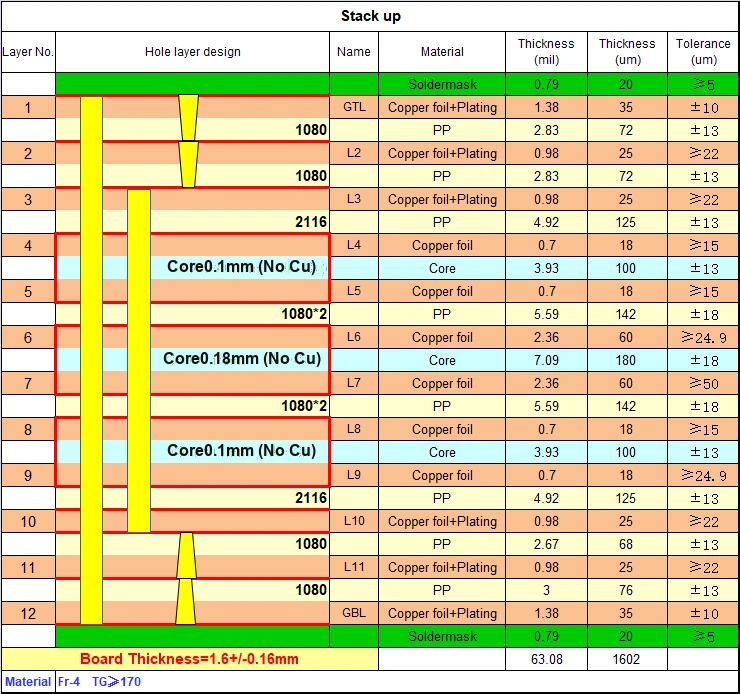
Dielectric adds up to 1,338 µm and finished copper to 260 µm, for a 1,598 µm layer sum – a 1.6 mm ± 0.16 mm finished board. The stack is symmetric: copper weights, dielectric thicknesses and build-up counts mirror about the center line, which keeps warp and layer-to-layer registration inside the laser-drill tolerance after two press cycles.
Impedance Targets on This 12-Layer 2-Stage Build
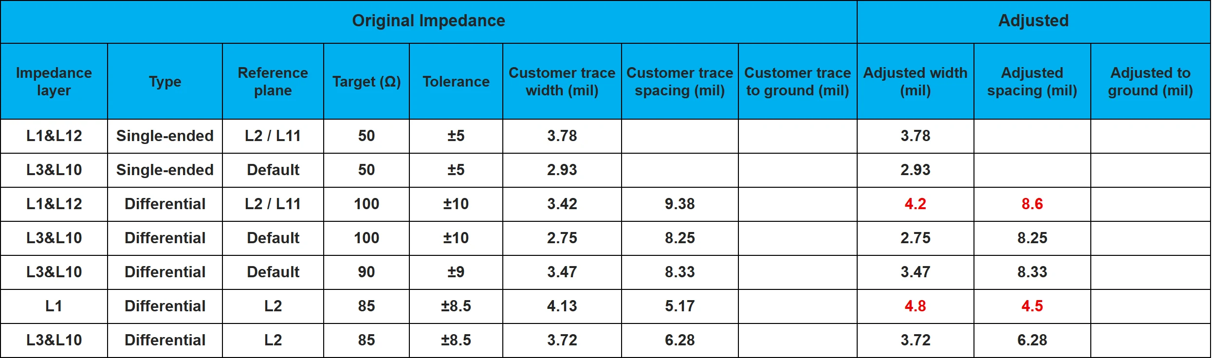
The impedance report for this 12-layer 2-stage HDI PCB models 50 Ω single-ended pairs on L1/L12 (referenced to L2/L11) at ±5% and ±8%, plus inner 50 Ω pairs on L3/L10 and L5/L8 at ±10%; differential pairs run at 85 Ω ±8%, and 90 Ω and 100 Ω at ±8% on the outer build-up and ±10% on the core layers.
Line geometry is tuned layer by layer – 3.5 to 4.4 mil for the 50 Ω single-ended pairs, and 3.4 to 4.8 mil line with 4.8 to 7.8 mil space for the differential pairs – and every adjusted width is documented against your original CAD figures in the report. A TDR coupon on each panel is measured and ships with the lot.
A 12-layer 2-stage HDI PCB needs one more decision than a standard multilayer board: the reference plane for each high-speed channel has to be reachable from the build-up. Because only L1 and L12 carry the fine geometry, camera SerDes and DDR pairs usually reference L2 or L11; routes that need a deeper plane drop through a buried via instead, which costs a stub. Defining that split before layout is cheaper than fixing it after the first coupon run.
Technical Specifications for a 2+8+2 HDI Stackup
| Parameter | Specification | Notes |
|---|---|---|
| Layer count | 12 layers, 2-stage HDI (2+8+2 build-up) | Two laser stages per side |
| Base material | FR-4 Tg 170 °C, Td > 340 °C | Lead-free reflow qualified |
| Board thickness | 1.6 mm ± 0.16 mm | Finished, symmetric stack balance |
| Panel size | Up to 500 × 600 mm | Array delivery with V-cut or mouse-bite |
| Outer copper | 35 µm (1 oz foil + plating) | Finished copper on L1 / L12 |
| Inner copper | 18-25 µm (0.5-0.75 oz) on L2 to L11; 60 µm (1.5 oz) heavy copper on L6 / L7 | L2 to L11 |
| Min laser blind via | 0.10 mm (4 mil) | L1-L2 / L2-L3 and L11-L12 / L10-L11 |
| Min buried via | 0.20 mm (8 mil) | Mechanically drilled L3-L10 sub-stack |
| Min through hole | 0.20 mm (8 mil) | Through L1-L12 |
| Line / space | 2.5 / 2.5 mil (63.5 µm) outer | 3 / 3 mil on inner layers |
| Min BGA pitch | 0.2 mm (8 mil) | Via-in-pad, microvia copper filled |
| Via fill | Resin plugged, or copper filled with plated over pad | Non-conductive or conductive fill |
| Impedance control | 50 Ω SE; 85 / 90 / 100 Ω differential | Per-panel TDR coupon; ±5% to ±10% by layer |
| Surface finish | ENIG 1-2 µ” gold / 120-240 µ” nickel | Immersion silver, OSP and lead-free HASL on request |
| Solder mask | LPI, color customer-specified | Matte or gloss |
| Silkscreen | Epoxy ink, color customer-specified | Single or both sides |
| Operating temperature | -40 °C to +125 °C | Automotive ambient range |
| Lead-free reflow | Peak 260 °C compatible | Verified per lot |
| Acceptance standard | IPC-A-600 Class 3 | IPC-6012 Class 3 build standard |
| Quality system | ISO 9001:2015, IATF 16949 | UL 796 recognized laminate systems |
Why Automotive Cockpit Controllers Move to a 12-Layer 2-Stage HDI Stack
A cockpit domain controller concentrates what used to be four or five ECUs: multi-display output, surround-view camera inputs, an AI co-pilot accelerator and the vehicle gateway. The SoC that runs it is a 0.2 mm-pitch BGA with several hundred balls, and that pitch is what decides the board, not the layer count. A 12-layer 2-stage HDI PCB routes those balls out through two laser microvia stages on each side, so the escape pattern never has to compete with the power planes underneath it.
The 2+8+2 notation describes how a 2 stage HDI PCB is laminated, not how it is drawn. The center eight layers stay a conventional sub-stack with mechanically drilled buried vias; only the outer two layers on each face are laser-drilled build-up.
That split is the reason a two-stage stack can still carry eight layers of ground and power planes: the planes stay in the thick core, where copper weight and low-impedance return paths are cheap, and the fine geometry stays in the thin dielectric where 0.10 mm laser vias are reliable.
The trade-off is real. Two sequential lamination cycles mean more process steps, more stack-balance discipline and a longer qualification cycle than a 1-stage build such as our 12-layer 1-stage HDI PCB.
If your SoC escapes at 0.4 mm pitch the 1-stage stack is the cheaper answer, and if the design needs fewer planes the 10-layer 2-stage HDI prototype covers that layer count on the same two-stage principle. Where the buried-via window has to be deeper, for example a 2+10+2 build on a thicker core, the 14-layer 2-stage HDI prototype covers that variant.
Key Advantages of 2-Stage HDI for Cockpit Controllers
- 0.2 mm-pitch fan-out without a third lamination cycle. Two laser stages handle the BGA escape; the buried-via window stays in the core, so the third press cycle a 3-stage build would need is never billed.
- 0.10 mm laser microvias with a 1:1 aspect ratio. Via reliability comes from drilling a thin dielectric, not from drilling a small hole through a thick one.
- 2.5/2.5 mil outer traces at 1 oz finished copper. Fine enough for dense escape routing, heavy enough that the power planes do not need a separate build-up.
- Buried vias mechanically drilled through the L3-L10 window. Deeper routing does not consume surface area, and the core sub-stack keeps its own sub-assembly inspection step.
- Symmetric stack. Mirror-image build-up and copper balance hold the board flat through two press cycles and lead-free reflow.
- Per-panel impedance coupons. TDR data for 50 Ω single-ended and 85 / 90 / 100 Ω differential ships with the lot instead of being assumed from the design.
- Via-in-pad with copper-filled microvias. The 0.2 mm BGA lands stay flat enough to place paste, so no via-in-pad escape is excluded on process grounds.
- One process window from prototype to volume. The lamination profile and prepreg lot are held, so the validation build and the production order are built on the same stack.
Overcoming Critical Challenges in 12-Layer 2-Stage HDI Design
1. 0.2 mm-Pitch BGA Fan-Out Inside a 2+8+2 Build
A 0.2 mm-pitch array on a 12-layer board usually fails on escape budget, not on layer count. Two microvia stages give each ball one via and one routing channel on L1, with the stage-2 via dropping to L3 for anything that has to reach the core. The limit we work against is annular ring and via-to-via clearance on L2: a 0.10 mm via with a 0.05 mm landing ring leaves roughly 0.20 mm of pitch budget, which is why the L2 prepreg stays thin and the drill-to-copper registration on that layer is controlled separately.
Designs that need two channels per ball at 0.2 mm pitch are a 3-stage problem rather than a 2 stage HDI PCB problem, and we will say so at the DFM stage rather than after the first build.
2. High-Speed Channels on a Mixed Reference Stack
Camera SerDes, DDR and PCIe Gen 3 pairs on a cockpit board all want a solid reference plane, and the 2+8+2 build only offers L2 and L11 close to the surface. The normal practice is to reference the build-up pair (L1 over L2) for the escape section, then transition to the core layers where the channel runs long. Every transition costs a stub and a controlled-impedance change, so the layout has to be planned layer by layer.
We review the stackup and the channel list together and flag the pairs whose reference changes mid-route before release.
3. Thermal and CTE Management from -40 °C to +125 °C
A cockpit board sees dashboard temperatures and its own SoC load in the same life. A Tg 170 °C laminate keeps the Z-axis expansion low enough that 0.10 mm microvias and 0.20 mm buried vias survive repeated reflow and thermal cycling, and the symmetric 2+8+2 build keeps the two build-ups moving together.
Copper balance matters more than the laminate grade here: an unbalanced stack warps during press and then shows up as microvia barrel cracking later, which is why we control copper distribution per layer rather than only at the outer faces.
Stacked vs Staggered Microvias in a 2+8+2 Sequential Lamination
A 2+8+2 build can be laminated with the two top microvias stacked or staggered. Stacked vias put the L2-L3 via directly on top of the L1-L2 via, which frees surface area but requires resin plugging and copper filling on the lower via plus tighter drilling registration. Staggered vias offset the second stage, which relaxes the fill requirement and is the default for this stack. Which one a design needs follows from the BGA pitch and how many signals have to leave each ball.
| Via configuration | What it costs | When it is the right answer |
|---|---|---|
| Staggered microvias | Offsets the stage-2 via; one extra routing grid around the via stack | Default on this 2+8+2 build; 0.2 mm BGA escape with a single channel per ball |
| Stacked microvias with copper fill | Copper-filled stage-1 via, plated over; tighter registration control | Rows of adjacent balls that all need to reach L3 or deeper directly under the pad |
| 3-stage build-up (2+8+2 no longer enough) | One extra lamination cycle and one extra laser stage | Denser than 0.2 mm pitch, or two escape channels per ball |
Laminate Selection for an Automotive 12-Layer 2-Stage HDI PCB
The default laminate for this automotive cockpit PCB stack is FR-4 Tg 170 °C with a decomposition temperature above 340 °C, which covers lead-free reflow and the -40 °C to +125 °C range without changing the impedance model. Where the board also carries a low-loss channel, we build the same stack on mid-loss and low-loss material – TU-872 SLK, EM-370(Z), IT-180A and MEGTRON 6 are the grades we stock most often – and re-tune line width and spacing on L1 and L12 to hold the impedance targets on the new Dk.
Halogen-free programs are built on S1150G (Tg 150), which is the grade to specify when the customer environmental requirement rules out brominated FR-4. Because S1150G has a lower Tg than the default laminate, the stack is re-dimensioned rather than copied. The general laminate comparison – Tg, Td, Dk, Df and cost ranking across grades – is in our PCB materials and laminates guide, and the interaction between via geometry and material choice is covered in the HDI PCB technology guide.
For reference, the default FR-4 Tg 170 system shows a typical Dk (dielectric constant) of 4.2 and a typical Df (dissipation factor) of 0.018 at 1 GHz. The mid-loss and low-loss grades we stock step down from there, and that step is what buys insertion-loss margin on a long SerDes run.
How Every 12-Layer 2-Stage HDI Panel Is Inspected
- Incoming laminate and prepreg control. Lot, Tg and Dk are recorded before the sub-stack is pressed, so a coupon result can be traced back to the material lot.
- Buried-via sub-assembly test. The L3-L10 core is drilled, plated and electrically tested before build-up lamination, so a buried-via defect is caught before it becomes unrepairable.
- Automated optical inspection after each imaging step. Inner layers, sub-stack and both outer layers are inspected separately, and the 2.5/2.5 mil geometry is verified on the film-to-board comparison.
- Flying-probe and fixture electrical test. 100% electrical verification on the finished panel, with net-list comparison against the Gerber source.
- Impedance coupon TDR. A coupon on every panel is measured for 50 Ω single-ended and 85 / 90 / 100 Ω differential and reported with the lot.
- Micro-section. A cross-section from the panel is polished and measured for microvia fill, barrel copper, dielectric thickness and layer registration.
The build acceptance is IPC-A-600 Class 3, and the shop runs a documented quality system to ISO 9001:2015 and IATF 16949. If your program needs the inspection record package and the coupon data attached to the shipment, say so on the order – the data exists per lot, and packing it costs nothing extra. Our PCB manufacturing services page lists the full flow, and manufacturing capability covers the equipment behind it.
Automotive Cockpit PCB Applications
- Cockpit domain controllers. One board for multi-display output, camera input and the gateway, with the SoC and its DDR on the same 2+8+2 stack.
- Digital instrument clusters. High-layer boards where the display driver, the graphics accelerator and the safety-relevant indicator logic share one assembly.
- AR-HUD controllers. Projection engines need the same fine-pitch fan-out plus a controlled-impedance path to the display interface – see our automotive HUD PCB page for the lower-layer variant.
- ADAS camera and sensor-fusion modules. Image-processing SoCs that need more escape layers than a 6- or 8-layer board can offer.
- In-cabin monitoring ECUs. Camera and radar data entering a single board where 0.2 mm-pitch BGA and fine traces have to coexist with power planes.
- Zonal gateways and central compute. Boards that route between vehicle domains and therefore need both high-speed channels and heavy copper distribution – comparable in demand to our automotive high-speed backplane PCB.
- Lower-complexity automotive programs. Where the SoC has fewer pins or the display count is smaller, our 6-layer automotive PCB prototype covers the same quality system on a conventional stack.
The same stack is also used outside automotive wherever a 0.2 mm-pitch SoC has to fan out at 12 layers; if your design is not automotive, the laminate and acceptance level change but the build-up and via rules do not. A control-and-computing version of the same build is documented on our 12-layer 2-stage HDI core board page. See the HDI PCB category for the rest of the range, or ask us for the same capability sheet you would request from any automotive PCB supplier.
How We Build Your 2+8+2 HDI Stackup
- DFM review against the stackup. We check the BGA pitch, escape budget, via-to-via clearance on L2, copper balance and annular ring before quoting the stack. If a design needs three stages, we say so here.
- Stackup and impedance proposal. We return a layer table with dielectric thicknesses, copper weights and a line-width / spacing recommendation per impedance target, so layout can start from the real build.
- Sub-stack lamination and buried-via drilling. The L3-L10 core is drilled, plated, resin processed where required and electrically tested.
- Build-up lamination, laser drilling and filling. Two sequential press cycles with 0.10 mm laser drilling and copper or resin fill on the microvias.
- Fine-line imaging at 2.5/2.5 mil. Outer-layer imaging and etching on 1 oz finished copper, followed by solder mask, legend and ENIG.
- Electrical test, coupon TDR and cross-section. Panel-level electrical test plus the per-panel impedance coupon and micro-section record.
- Array and packaging. V-cut or mouse-bite array, vacuum packing with the inspection record.
Files we need to start: Gerber RS-274X or ODB++ (Ucamco Gerber reference), the stackup requirement or a target thickness, impedance targets with the net list, BGA pitch, surface finish and any mechanical outline. If there is no stackup yet we propose one from the BGA pitch and layer count at no charge, and we return DFM feedback in writing with the quote.
Prototype turnaround for a 12-layer 2-stage build is typically 5-7 working days for small quantities, confirmed at engineering review, and low-loss laminates add material sourcing time. Every panel is built and inspected to the IPC-A-600 and IPC-6012 Class 3 acceptance criteria, and the coupon and micro-section records ship with the lot.
Why Choose Season PCB as Your HDI PCB Manufacturer
- HDI is a core process, not an outsourced step. 1-stage, 2-stage and any-layer build-ups run in the same shop as the standard multilayer work, so the lamination profile does not change hands mid-build.
- Capacity behind the prototype. 998PCB Group has manufactured since 2006, with 3,000,000 m² of annual capacity across plants in Shenzhen, Jiangxi and Anhui, and a 2-30 layer range.
- Quality system built for automotive programs. ISO 9001:2015 and IATF 16949 quality systems, IPC-A-600 Class 3 acceptance, UL recognized laminate systems, RoHS and REACH compliance.
- Engineering contact, not a ticket queue. The same engineer who reviews the stackup answers questions during fabrication.
- Turnkey option. Bare board, or board plus assembly – see PCB manufacturing services for how the two are split.
As an HDI PCB manufacturer, Season PCB builds 12-layer 2-stage HDI PCBs for automotive PCB programs – cockpit domain controllers, instrument clusters, AR-HUD projection engines and ADAS sensor-fusion modules – and for any 0.2 mm-pitch SoC that has to fan out at 12 layers. The build is quoted, engineered and inspected in one shop, on one lamination profile, from prototype quantities to series production.
Frequently Asked Questions
What is a 12-layer 2-stage (2+8+2) HDI PCB?
It is a 12-layer board built with a sequential lamination process: two laser-drilled build-up layers on the component side, an eight-layer core sub-stack with mechanically drilled buried vias, and two matching build-up layers on the solder side. The build-up gives the fine geometry and the 0.10 mm microvias, while the core keeps the ground and power planes in heavier copper.
What does the 2+8+2 notation actually describe?
The three numbers are layer counts, not via counts: 2 build-up layers on top, 8 core layers in the middle, 2 build-up layers on the bottom. Some suppliers write the same stack as 2+n+2, where n is the core layer count. That makes 12 copper layers in total, with two microvia stages per side – L1-L2 and L2-L3 on the top, L12-L11 and L11-L10 on the bottom.
Why does a cockpit controller need HDI instead of a standard 12-layer board?
A 0.2 mm-pitch BGA cannot fan out on a board that only has plated through holes, because each ball needs an escape via and a routing channel that a through hole cannot provide at that pitch. The build-up layers give the escape and the 12-layer core gives the planes and the routing channels underneath, which a 6- or 8-layer HDI board cannot match.
Which laminate should I specify for -40 °C to +125 °C operation?
FR-4 Tg 170 °C with a decomposition temperature above 340 °C is the default for this stack and covers lead-free reflow plus the automotive ambient range. If a high-speed channel needs lower loss we re-build the same stack on TU-872 SLK, EM-370(Z), IT-180A or MEGTRON 6 and re-tune the impedance. Halogen-free programs use S1150G (Tg 150).
What are the smallest via and trace geometries you hold on this stack?
0.10 mm laser blind vias in the two build-up stages, 0.20 mm mechanically drilled buried vias through the L3-L10 window, 0.20 mm minimum through holes, and 2.5/2.5 mil line and space on the outer layers with 3/3 mil on the inner layers.
How do you control impedance on a 12-layer 2-stage build?
We tune line width and spacing against the reference planes on L2 and L11 for the outer layers, and against the core planes for inner routing. 50 Ω single-ended and 85 / 90 / 100 Ω differential are standard, and a TDR coupon on every panel is measured and reported with the lot.
What files do you need for a DFM review and quotation?
Gerber RS-274X or ODB++ data, the stackup requirement or a finished-thickness target, impedance targets with the associated nets, BGA pitch, surface finish and the mechanical outline. Without a stackup we propose one from the BGA pitch and layer count, and we return DFM feedback in writing with the quote.
Can the same stack be used for volume production?
Yes. The lamination profile, prepreg lots and impedance model from the validation build are held for the production order, so the volume boards come off the same process as the prototypes. Moving from a small validation batch to serial quantities does not require a re-qualification of the stackup.
How is a 12-layer 2-stage HDI PCB priced?
Cost on this stack is driven by three things rather than by layer count: the two sequential lamination cycles, the microvia count and stack pattern, and the laminate grade. A 2+8+2 build uses the same press capacity as a 12-layer through-hole board but adds two build-up cycles, so panel utilisation moves the number more than the layer count does. We return a fixed quotation with the DFM review rather than a per-square-metre rate.
Do you build the same stack for non-automotive programs?
Yes. Outside automotive the build-up and via rules do not change; what changes is the laminate grade and the acceptance level. A consumer or industrial program can run the same 2+8+2 stack with a Tg 150 laminate and Class 2 acceptance, while an automotive program keeps Tg 170 and Class 3. The coupon set and the micro-section report ship either way.
Ready to Start Your 12-Layer 2-Stage HDI PCB Project?
Send the Gerber data, the stackup requirement and the impedance targets, and we will return a DFM review with the layer table and a quotation. If the 0.2 mm-pitch escape budget looks like a three-stage problem, you will hear that at the review stage rather than after the first build.