Book Appointment Now

Plating voids in microvias explained: point vs seam voids, the mechanisms behind them, and the chemistry, pulse plating and agitation fixes that remove them.
Plating Voids in Microvias: Root Causes and How Factories Fix Them
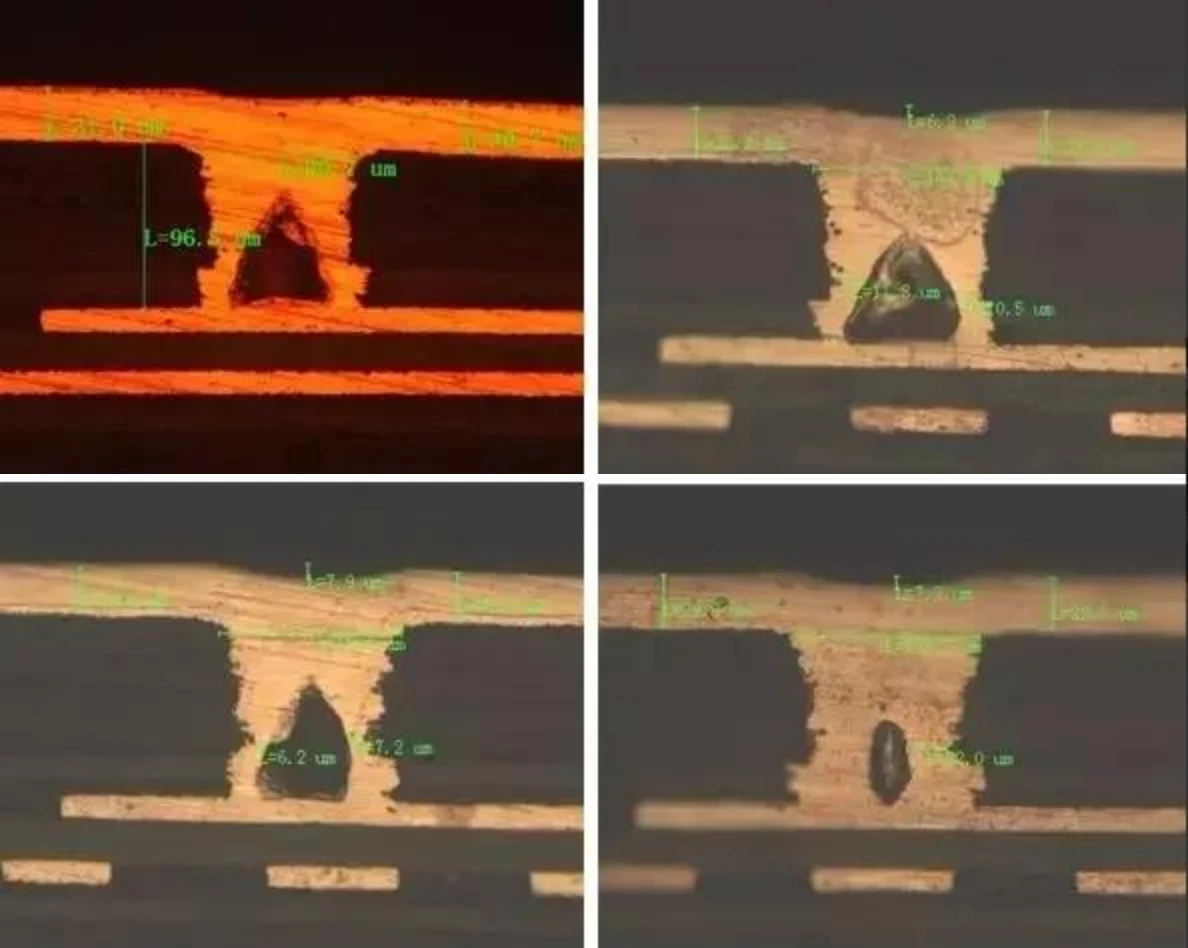
A copper-filled microvia can look flawless on the surface and still hide a cavity inside the barrel. These plating voids in microvias are among the most expensive defects in HDI production because they stay invisible until cross-section or X-ray inspection — by which time an entire panel, not just one via, may be in question. Worse, the ones that escape detection surface later as thermal-cycling failures in the field.
This guide explains where the voids actually come from — hydrogen entrapment, mass-transfer limits and additive imbalance — and walks through the levers that remove them: bath chemistry, pulse plating, agitation hardware and in-process monitoring, ending with a case where the void rate fell from 30% to under 4%.
Table of Contents
- What Are Plating Voids in Microvias
- Why a Tiny Cavity Threatens the Whole Assembly
- What Causes Plating Voids in Microvias
- Bath Chemistry: Tuning the Additive Triangle
- Current Density and Pulse Plating
- Agitation and Equipment: Breaking the Mass-Transfer Bottleneck
- Process Monitoring: From Sampling to Prediction
- Case Study: Cutting the Void Rate From 30% to Under 4%
- What to Ask a PCB Supplier About Via Filling
- FAQ
- Get Your Fill Rules Reviewed Before You Order
What Are Plating Voids in Microvias
Copper-filled vias are the structural backbone of modern HDI. Laser-drilled microvias are plated not merely lined but solidly filled with copper, so that one via can be stacked on another in high-density HDI constructions, and so the barrel doubles as a short thermal path. A filled via is a copper rivet; a void is the flaw that turns the rivet back into a tube.
Voids come in two families with very different fingerprints. Point voids are isolated spherical or elliptical pores, usually near the base of the fill. Seam voids — sometimes called ringing voids — run along the barrel wall as a continuous or semi-continuous gap. The distinction matters because the two families have different root causes and respond to different fixes, which is the first thing a failure analyst checks when a cross-section lands on their desk.
The stakes scale with the stackup. In a 2-stage or 3-stage HDI build, each stacked via sits on top of the fill below it; a void in a lower via becomes the foundation crack for everything plated above it. That is why via-filling capability, not laser drilling alone, is the practical ceiling on how aggressively a fabricator can stack.
Why a Tiny Cavity Threatens the Whole Assembly
The obvious problem is electrical. A void changes the effective cross-section of the interconnect, and where the copper narrows, current crowds and resistance rises. In power delivery paths the void becomes a hot spot; in signal paths it acts as an impedance discontinuity that reflects energy — a real problem for the multi-gigabit edges that HDI stackups exist to carry in the first place.
The less obvious problem is mechanical. Copper expands about an order of magnitude more than the surrounding dielectric with temperature, so every thermal cycle squeezes the filled barrel. A void concentrates that cyclic stress at its edges, where cracks nucleate and then propagate through the remaining copper until the connection opens or drifts high-ohmic. A board that passes final test can therefore still fail in the field at cycle counts the design never budgeted for.
There is also a thermal dimension: copper conducts heat roughly three orders of magnitude better than laminate, so a void in a thermally-motivated via removes exactly the path the via was placed there to provide. Reliability frameworks from IPC — now the Global Electronics Association — treat filled-via integrity accordingly, and the economics follow: a void found at cross-section scraps a panel, while one found in the field scraps a customer relationship.
What Causes Plating Voids in Microvias
Voids are not random bad luck; each family has a mechanism that is well understood and, more importantly, preventable.
| Void family | Typical location | Dominant mechanism | Primary detection |
|---|---|---|---|
| Point void | Isolated sphere or ellipse near the via base | Hydrogen bubble nucleates on the hole wall, cannot escape against surface tension, and copper grows around it | Cross-section; X-ray sampling |
| Seam (ringing) void | Continuous or semi-continuous gap along the barrel wall | The via mouth closes early while the base still needs copper — a current-distribution and mass-transfer failure | Cross-section at mid-barrel height |
Point voids start with hydrogen. In acid copper plating, hydrogen reduction at the cathode is an unavoidable side reaction of copper deposition, and it accelerates at high current density or low bath pH. Inside a narrow, high-aspect-ratio hole, a bubble that nucleates on the wall has almost no buoyant escape path: surface tension and viscous drag pin it in place while copper deposits around it, sealing the bubble in as a permanent pore.
Seam voids start with current geometry. Current follows the path of least resistance, so the via mouth — facing the bath directly — plates much faster than the via base. The mouth narrows into a V-shaped throat, fresh electrolyte rich in copper ions and additives can no longer reach the bottom, and the interior becomes a mass-transfer dead zone. Additive imbalance then makes things worse: large-molecule suppressors diffuse slowly and pile up near the mouth, while the small-molecule accelerator the base needs runs short exactly where deposition should be fastest. The mouth seals over an unfinished fill, and the ring-shaped gap is locked in.
Bath Chemistry: Tuning the Additive Triangle
Modern via filling runs on three organic additives working in concert, each doing a spatially distinct job. Suppressors — typically polyethylene glycol (PEG) — blanket the high-current-density regions around the via mouth and slow deposition there. Accelerators — sulfonate species such as SPS — survive diffusion into the via base and push bottom-up growth. Levelers adsorb strongly at the mouth and flatten the emerging surface. Get the balance right and the via fills from the bottom up like a well-poured casting; get it wrong and the mouth skins over first.
The supporting cast matters as much as the lead actors. Inorganic benchmarks in a typical acid copper bath run in these bands: sulfuric acid around 180–220 g/L for conductivity without attacking dry film, copper ions around 60–80 g/L for deposition rate without sacrificing throwing power, and chloride at a seemingly trivial 50–80 ppm — yet chloride is the bridge that lets suppressor, copper and the electrode surface form the working complex. A bath can be chemically “in spec” on copper and acid and still fill badly if the additive ratios have drifted.
One practical insight from production: molecular weight is a design variable, not a datasheet footnote. A lower-molecular-weight suppressor diffuses faster, which narrows the concentration gradient between mouth and base. Swapping a heavy suppressor for a lighter grade is often the single highest-leverage chemistry change available when seam voids dominate — a lever the case study below uses directly.
Current Density and Pulse Plating
Current density is the most sensitive knob in the whole process. High current density raises throughput but amplifies both hydrogen evolution and the mouth-versus-base current imbalance. The production pattern that works is counterintuitive: plate slower. For blind vias above roughly 5:1 aspect ratio, a soft start around 0.5–0.8 ASD lets copper establish at the base before the current ramps toward 1.5–2.0 ASD for bulk filling — trading minutes of bath time for a fundamentally lower void probability.
Pulse plating turns that passive trade-off into active control. Instead of a constant current, the waveform alternates a forward pulse, during which copper deposits, with a reverse pulse, during which the current briefly reverses. The reverse phase does three useful things at once: adsorbed hydrogen detaches and escapes, depleted copper ions and additives at the via base are replenished, and the over-plated mouth receives a slight electrochemical etch that reopens the throat before it can seal.
Frequency, duty cycle and reverse ratio are tuned per via structure and bath system — there is no universal waveform. As a scale reference, deep structures such as 8:1 through-silicon vias are routinely run with forward pulses around 1.5 ASD for 10 ms and reverse pulses around 0.5 ASD for 1 ms. PCB microvias sit at shallower aspect ratios than that, which is exactly why pulse plating plus correct chemistry can push a filled blind via to near-zero voids.
Agitation and Equipment: Breaking the Mass-Transfer Bottleneck
No chemistry survives a starved via. Conventional air agitation stirs the bulk bath but does little for the boundary layer inside a 100 µm hole. Directed jet plating solves this by aiming pressurized electrolyte at the panel surface, driving fresh solution into the via mouths; pressure, angle and flow are programmable, which turns mass transfer from an accident of geometry into a set parameter.
Ultrasonic agitation attacks the hydrogen problem directly. Cavitation micro-bubbles collapsing near the hole wall blast adhered hydrogen off the surface and violently refresh the local solution. Reported results on high-aspect-ratio blind vias put the void-rate reduction above 60% with ultrasonics in the 40 kHz range at power densities of roughly 1–2 W/cm² — a large gain for a retrofit-level change.
Equipment architecture completes the picture. Horizontal conveyorized plating lines move panels through the bath on their edge, giving both faces a symmetric, well-controlled flow field — an advantage for thin panels and large formats where vertical flooding is uneven. None of these machines compensates for wrong chemistry, but the reverse is also true: the best additive package underperforms in a bath that cannot feed the hole.
Process Monitoring: From Sampling to Prediction
Traditional control of plating voids in microvias is retrospective: cross-section coupons and X-ray images tell you what already happened. Modern lines increasingly watch the plating process itself, because the precursors of voids — additive depletion, bath drift, current imbalance — are measurable in real time.
| Method | Destructive? | What it catches |
|---|---|---|
| Cross-section | Yes (coupon) | Point and seam voids, fill height and dimple depth — the acceptance reference |
| X-ray inspection | No (sampled) | Larger internal voids across a production panel without cutting it |
| Electrochemical impedance spectroscopy (EIS) | No (in-bath) | Additive depletion and surface-state drift that precede voids |
| Optical reflectometry | No (in-line) | Fill progress in transparent substrates such as glass interposers |
EIS deserves a note because it closes the loop on chemistry: by measuring the bath’s impedance response to a small AC perturbation, changes in additive concentration and electrode surface state show up as shifts in charge-transfer resistance — the same quantities that determine whether the via mouth suppresses and the base accelerates. Feeding those readings back into dosing keeps the additive triangle inside its window instead of discovering the drift on next week’s coupon.
The current frontier is predictive: line sensors for temperature, pH, current density and bath impedance, correlated with historical defect data, can train models that flag an approaching void condition and adjust parameters — lower current, more agitation — before a single defective via exists. This is where the industry’s zero-defect ambitions actually live, and fabricators investing in it treat fill data as process IP.
Case Study: Cutting the Void Rate From 30% to Under 4%
A production case makes the mechanisms concrete. A customer board for 5G base-station electronics carried a dense field of blind microvias at 50 µm diameter and roughly 2:1 aspect ratio. Initial trials on DC plating produced a void rate near 30% — far outside the customer’s requirement of under 5% — with seam voids concentrated at mid-barrel height.
Cross-section analysis pointed to the two mechanisms described above: the suppressor had drifted too rich at the mouth, closing vias early, and the agitation could not keep the interior fed. The response touched all three levers at once — chemistry, waveform and equipment:
| Parameter | Before | After |
|---|---|---|
| Plating mode | DC plating, single current setting | Pulse plating: forward 1.2 ASD / 8 ms, reverse 0.4 ASD / 1 ms |
| Suppressor | PEG-8000 at 300 ppm | PEG-4000 (lower molecular weight) at 200 ppm |
| Accelerator | SPS at 2 ppm | SPS raised to 3 ppm to strengthen bottom-up growth |
| Agitation | Air agitation only | Directed jet flow plus 40 kHz ultrasonics during the first five minutes |
| Microvia void rate | ≈ 30% | Below 4% |
The result was a void rate below 4% with fully rounded fill profiles and flat surfaces, and the boards went on to pass 1,000 thermal cycles from −40 °C to +125 °C. The instructive part is not any single change — a lighter suppressor alone or pulse plating alone would have left voids — but that the failure was a system property of chemistry, waveform and mass transfer, and so was the fix. The same discipline is what a fabricator applies when qualifying demanding builds such as a 10-layer 2-stage HDI prototype, where stacked vias multiply the cost of every void.
What to Ask a PCB Supplier About Via Filling
Plating voids in microvias rarely announce themselves in a quotation PDF, so the burden falls on asking the right questions before the order, not after the failure. A short, effective list:
- Do you cross-section fill coupons per lot, and can you share representative images at my aspect ratio?
- Is your fill process pulse plating or DC, and what reverse ratio do you run for my via structure?
- How do you monitor and dose the additive system — fixed schedules or bath-analysis driven?
- What is your standard X-ray sampling plan for filled vias on production panels?
- Which acceptance criteria govern fill height and voids — IPC-6012 class requirements or my drawing’s note?
Suppliers with genuine capability answer these from process data rather than from marketing copy. The IPC qualification standards — IPC-6012 for rigid board performance among them — give buyers a shared vocabulary for class-level acceptance, but the differentiator between suppliers is how tightly they hold the process window between coupons, not which standard they cite. For stacked, any-layer constructions such as a 14-layer 2-stage HDI prototype or a 10-layer HDI industrial control PCB, that window discipline is precisely what you are buying.
Frequently Asked Questions
What does a plating void in a microvia look like?
In a cross-section, a point void appears as an isolated round or elliptical pore inside the copper fill, usually near the base of the via. A seam void shows as a dark, continuous or broken line running along the barrel wall. On an X-ray image, larger voids read as lighter spots inside the via positions. Both families are invisible from the board surface, which is why sampling and sectioning matter.
Are voids in copper-filled vias always a reject?
It depends on size, location and the acceptance class your drawing invokes. Small, isolated porosity away from the barrel wall may be acceptable under class-level criteria, while a seam void or any void in a stacked-via interface is normally grounds for rejection. The practical rule: define void acceptance explicitly in the fabrication drawing, referencing IPC-6012 class requirements, instead of leaving it to the supplier’s default.
Why do seam voids form along the via wall instead of the center?
Because the via mouth plates faster than the base. Current crowds at the opening, the mouth narrows into a V-shape, and fresh electrolyte with copper ions and additives can no longer reach the bottom. The base stops receiving enough accelerator while suppressors enrich near the mouth, deposition there stalls, and the partially filled barrel seals over — leaving a gap along the wall.
Does pulse plating guarantee a void-free fill?
No. Pulse plating substantially reduces void risk because the reverse pulse releases hydrogen, replenishes the via base and lightly etches the over-plated mouth, but it works together with correct additive ratios and adequate agitation. A void produced by starved mass transfer can survive a perfect waveform. The reliable combination is pulse plating plus tuned chemistry plus directed flow, verified by cross-section data.
How are plating voids detected before shipment?
Two ways. Cross-sectioning a process coupon from each lot is the destructive reference — it shows voids, fill height and dimple depth. X-ray inspection is non-destructive and samples production panels for larger internal voids. Leading lines add in-bath electrochemical impedance monitoring, which flags additive depletion and bath drift before they produce voids at all, turning detection from inspection into prevention.
Does a higher aspect ratio increase void risk?
Yes, strongly. The deeper and narrower the via, the harder it is for solution and additives to reach the base and for hydrogen to escape, and the more the mouth-to-base deposition imbalance grows. Most HDI laser microvias run near a 1:1 aspect ratio, which is comfortably within proven filling windows; as the ratio climbs, void control — not laser drilling — becomes the practical limit on the structure.
What should I include in a via-filling specification?
Specify via diameter, target aspect ratio and which vias must be filled, the required fill class and acceptance criteria for voids, fill-height or dimple limits if your assembly needs them, and the verification method — coupon cross-section frequency and X-ray sampling. Point to IPC-6012 for class-level performance, and add anything specific to stacking, such as requirements for the interface where a second via will be plated on top.
Get Your Fill Rules Reviewed Before You Order
The most reliable way to avoid plating voids in microvias is to confirm the fill window before the order: send your stackup, via sizes and aspect ratios, and the fill-capability review will show where your design sits against proven process data. For a broader view of how filled vias carry multi-stage builds, our cross blind-buried via HDI guide walks the full construction.