Book Appointment Now

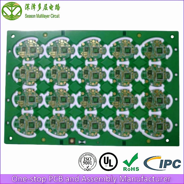
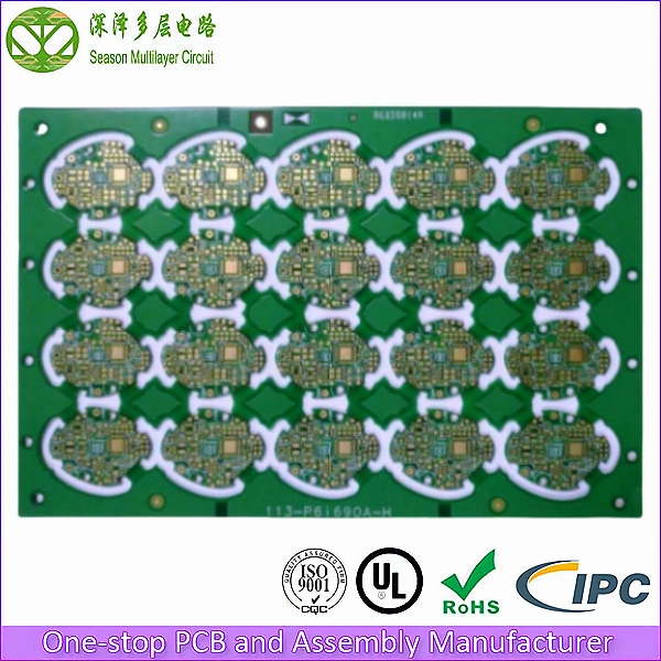
6-Layer 2-Stage HDI Headphone PCB
Advanced 2-stage HDI PCBs for premium wireless headphones — headphone PCB manufacturing with active noise cancellation (ANC), Bluetooth 5.3, high-resolution audio processing, and ultra-compact form factor for over-ear and in-ear designs.
Premium wireless headphones pack an incredible amount of technology into a compact space: ANC processors, Bluetooth SoCs, audio DACs, battery management, touch sensors, and multiple microphones — all requiring dense, high-speed PCB routing. At Season Multilayer Circuit, we manufacture 6-layer 2-stage HDI headphone PCBs with stacked microvias that deliver the density, audio signal purity, and reliability your headphone electronics demand.
6
Layer Count
2.5/2.5 mil
Min. Trace/Space
0.075 mm
Min. Via Diameter
Tg 180
Glass Transition Temp
1–2 µ”
ENIG Gold Thickness
ISO 9001:2015
ISO 14001
UL (E305905)
IPC Class 2 / Class 3
RoHS
6-Layer 2-Stage HDI Headphone PCB Stackup Diagram
Our 6-layer 2-stage HDI stackup for headphone applications uses sequential lamination with stacked microvias to achieve maximum routing density in the smallest possible form factor, supporting ANC processors, Bluetooth SoCs, and high-resolution audio circuitry.
- Top Layer (Copper/Plated): Fine-pitch BGA, audio codec, Bluetooth SoC, USB-C controller
- Inner Layer 2 (Ground Plane): EMI shielding and audio signal reference ground
- Inner Layer 3 (Signal Layer): High-speed audio data bus and Bluetooth RF routing
- Inner Layer 4 (Power Plane): Clean power distribution for audio DAC and ANC processor
- Inner Layer 5 (Signal Layer): Sensor routing and battery management signals
- Bot Layer (Copper/Plated): Bottom routing and thermal pad for battery charging
2-stage HDI uses two sequential lamination cycles, enabling stacked microvias that connect L1-L3 and L4-L6 independently. This doubles the routing density compared to 1-stage HDI, critical for fitting complete headphone electronics in compact earcup or earbud housings.
Technical Capability & Specifications
| Parameter | Specification | Advanced Capabilities |
|---|---|---|
| Layer Count | 6 Layer 2-Stage HDI | 2-32L (Mass); 2-64L (Sample) |
| Base Material | FR-4 S1000-2M Tg 180 | SY, NY, TUC, ZY, EMC, KB, ITEQ, Rogers, Megtron, Nelco, Isola |
| Board Thickness | 0.4mm | 0.2-6.4mm (Mass); 0.15-20mm (Sample) |
| Panel Size | 45x30mm/1 | 800x600mm (Mass); 1050×610 (Sample) |
| Copper Thickness | Outer: 1/2 oz Inner: 1/3 oz | Outer: 1/3–12 oz Inner: 1/4–12 oz |
| Min Drill Size | 0.075mm (Laser) | 0.050mm (Laser Sample) |
| Min Trace Width/Spacing | 2.5/2.5 mil | 2.0/2.0 mil (Sample) |
| Blind Via (Stage 1) | 0.075mm Laser | 0.050mm Laser (Sample) |
| Blind Via (Stage 2) | 0.075mm Laser | 0.050mm Laser (Sample) |
| Surface Finish | ENIG | HASL, OSP, Immersion Silver, Immersion Tin, ENIG, ENEPIG |
| Solder Mask | Green | Green, Black, Blue, Red, Yellow, White, Purple |
| Impedance Control | 50/90 Ohm +/-8% | +/-5% available for RF applications |
Key Advantages of Our Headphone PCB
- 2-Stage HDI for Maximum Density: Sequential lamination with stacked microvias enables 60% higher routing density than 1-stage HDI, fitting complete headphone electronics (ANC + BT + DAC + battery management) in ultra-compact earbud or earcup PCBs.
- Audio Signal Purity: Dedicated ground planes (L2, L5) isolate sensitive analog audio traces from digital switching noise, ensuring SNR >110dB for studio-quality sound reproduction.
- Bluetooth RF Optimization: Controlled impedance RF routing (50 ohm +/-8%) with optimized antenna feed lines ensures stable Bluetooth 5.3 connectivity at up to 30m range.
- Ultra-Thin Profile: 0.4mm board thickness fits within the slim internal geometry of modern over-ear and in-ear headphone designs without compromising structural integrity.
- Stacked Microvia Reliability: IPC Class 2 / Class 3 compliant stacked microvia processing with copper fill ensures long-term via reliability under thermal cycling and mechanical stress.
Overcoming Critical Challenges in Headphone Electronics Design
When sourcing HDI PCBs for premium headphone applications, engineers encounter three critical challenges. Here is how our engineering team eliminates them:
1. Audio Signal Degradation from Digital Noise
The Problem: Modern headphones integrate Bluetooth SoCs, ANC processors, and audio DACs on the same tiny board. Digital switching noise from Bluetooth and processing circuits couples into sensitive analog audio traces, causing hissing, pops, and reduced SNR that audiophiles immediately notice.
Our Solution: Our 2-stage HDI stackup uses dedicated ground planes (L2, L5) to create physical isolation between analog audio circuits and digital processing blocks. The inner power plane (L4) provides clean, filtered power to audio components. The result: SNR >110dB and THD <0.001% for studio-quality sound.
2. Component Density in Earbud Form Factors
The Problem: True wireless earbuds must fit a Bluetooth SoC, ANC processor, audio DAC, battery charger, multiple microphones, and antenna in a PCB smaller than a thumbnail. Standard HDI technology cannot route enough interconnects in this space.
Our Solution: Our 2-stage HDI process with 0.075mm laser-drilled stacked microvias enables 60% higher routing density than 1-stage HDI. Via-in-pad technology places interconnects directly under BGA pads, maximizing component placement density without adding board layers.
3. Bluetooth RF Performance in Metal Earcup Housings
The Problem: Over-ear headphones with aluminum or titanium earcup housings create RF shielding that blocks Bluetooth signals. Poor antenna feed line design causes weak connectivity, range reduction, and dropouts.
Our Solution: We provide 50 ohm controlled impedance routing for antenna feed lines with precise +/-8% tolerance. Our engineering team optimizes antenna keep-out zones and ground plane cutouts to maximize RF radiation efficiency through plastic windows in metal housings.
Where Our Headphone PCBs Are Used
Our 6-layer 2-stage HDI headphone PCBs power a wide range of audio applications:
- Premium Over-Ear Headphones: ANC-enabled wireless headphones with high-resolution audio processing and 40+ hour battery life.
- True Wireless Earbuds (TWS): Ultra-compact earbud PCBs fitting Bluetooth SoC, ANC, and battery management in a thumbnail-sized board.
- Gaming Headsets: Low-latency wireless gaming headsets with spatial audio processing and multi-microphone arrays.
- Hearing Assistance Devices: Medical-grade hearing aids and PSAPs requiring ultra-low-noise audio circuits and miniaturized form factors.
- Smart Audio Wearables: Smart headphones with voice assistant integration, health monitoring, and open-ear bone conduction designs.
Our Quality Guarantee for Headphone PCBs
Audio electronics demand exceptional signal quality and long-term reliability. We implement rigorous testing protocols on every board:
- 100% AOI Inspection: Automated Optical Inspection scans every layer for trace breaks, shorts, and microvia defects.
- 100% Electrical Testing (E-Test): Flying probe or fixture-based testing verifies continuity, isolation, and microvia integrity.
- Controlled Impedance Testing: Polar Instruments test report documenting 50/90 ohm compliance for RF and audio signal paths.
- Microvia Cross-Section Analysis: Sample cross-sectioning verifies stacked microvia copper fill quality and interconnect reliability.
- Certifications: ISO 9001:2015, ISO 14001, UL (E305905), RoHS compliant. IPC Class 3 available for premium audio.
Why Choose Season PCB for Your Headphone PCB?
With nearly 20 years of experience in PCB manufacturing, Season Multilayer Circuit has served over 8,000 global clients in consumer audio, wearable electronics, and telecommunications. Our three manufacturing facilities provide capacity for both rapid prototyping and high-volume production.
We understand that headphone electronics demand exceptional signal quality and miniaturization. That is why every 6-layer 2-stage HDI headphone PCB we ship is backed by:
- Free DFM file checking before production
- 24/7 dedicated engineering support
- Guaranteed on-time delivery
- No minimum order quantity — from 1 prototype to 100,000+ units
- Engineering fee waivers on bulk production orders
Season PCB specializes in 2-stage HDI headphone PCB manufacturing for premium wireless audio applications. Our headphone PCB products feature stacked microvias, audio-grade signal isolation, and Bluetooth RF optimization. Each headphone PCB meets IPC standards.
For your headphone PCB needs, Season PCB provides fast turnaround, competitive pricing, and ISO-certified quality. Contact us for headphone PCB manufacturing today.
Our headphone PCB boards comply with UL safety certifications and IPC manufacturing standards. Each headphone PCB undergoes signal integrity testing and microvia reliability verification. For volume production, the same stackup runs on 998PCB Group’s advanced HDI PCB lines at the group’s Shenzhen campus.
Frequently Asked Questions
What is the difference between 1-stage and 2-stage HDI?
1-stage HDI uses a single sequential lamination cycle with blind vias connecting the outer layer to one inner layer. 2-stage HDI uses two sequential lamination cycles, enabling stacked microvias that connect through multiple layer pairs independently. This doubles the routing density, critical for ultra-compact headphone PCBs.
Can you achieve SNR >110dB on headphone PCBs?
Yes. Our stackup uses dedicated ground planes to physically isolate analog audio circuits from digital switching noise. Combined with clean power plane filtering and careful component placement, we consistently achieve SNR >110dB and THD <0.001% on audio circuit boards.
What is the lead time for 2-stage HDI headphone PCB prototypes?
2-stage HDI requires two sequential lamination cycles, so standard prototype lead time is 10-12 working days. Expedited 7-day service is available. Mass production typically takes 18-22 working days.
What materials and surface finishes do you use for HDI headphone PCBs?
The standard build is FR-4 S1000-2M (Tg 180) at 0.4mm board thickness, with SY, NY, TUC, ZY, EMC, KB, ITEQ, Rogers, Megtron, Nelco, and Isola laminates available. Copper is 1/2 oz outer and 1/3 oz inner, and minimum laser drill is 0.075mm with 2.5/2.5 mil trace width and spacing. ENIG is the standard surface finish, with HASL, OSP, immersion silver, immersion tin, and ENEPIG optional, and controlled impedance is held to 50/90 ohm plus/minus 8 percent. Solder mask is green as standard, with black, blue, red, yellow, white, and purple available.
How do you verify quality on HDI headphone PCBs?
Every board passes 100% AOI, which scans each layer for trace breaks, shorts, and microvia defects, plus 100% electrical testing by flying probe or fixture to verify continuity, isolation, and microvia integrity. A Polar Instruments impedance test report documenting 50/90 ohm compliance for RF and audio signal paths accompanies every batch, and sample cross-sectioning verifies stacked microvia copper fill quality and interconnect reliability. We are certified to ISO 9001:2015, ISO 14001, UL (E305905), and RoHS, with IPC Class 3 available for premium audio.
Ready to start your Headphone PCB project?
Whether you need 5 pieces for prototyping or 50,000 for mass production, our engineering team is ready to support your headphone project with DFM review, impedance modeling, and fast-turn fabrication.
Tel: (+86) 18681528532 (WhatsApp)
E-mail: roc@season-pcb.com