Book Appointment Now

A 10-layer any-layer HDI PCB (ELIC) built with laser microvias on every adjacent layer pair, the full stackup table, lamination sequence and capability envelope.
10-Layer Any-Layer HDI PCB (ELIC) for Dense Control and Wearable Designs
An any-layer HDI PCB, also written ELIC, for every layer interconnection, is a board in which every adjacent layer pair is connected by a laser microvia, not only the outer pairs. On a conventional 1-stage or 2-stage HDI build the laser vias stop at a buried-via core; on any-layer HDI the interconnect continues straight through the stack, so a signal can step from L1 to L10 without a single through hole. This page documents the 10-layer any-layer HDI PCB we build as our reference ELIC design: nine laser via pairs, a 0.064 mm core, every dielectric held under 100 µm for a 1:1 blind-via aspect ratio, and a 0.8 mm finished thickness.
This any layer HDI PCB is laminated in five press cycles: the 0.064 mm core carries L5 and L6, and each later cycle adds one layer per side and closes two more via pairs. By the fourth cycle all nine pairs are complete. Below you will find the full stackup table with tolerances, the cycle-by-cycle lamination sequence, the capability envelope for production and sample runs, and the inspection records that ship with every batch of any-layer HDI PCB work.
Send the Gerber data and your target stackup for a DFM review, or start from the HDI PCB technology guide if you are still comparing any-layer HDI against 2-stage and 3-stage alternatives. For a 2-stage point of comparison at the same quality level, see the 10-layer 2-stage HDI prototype PCB.
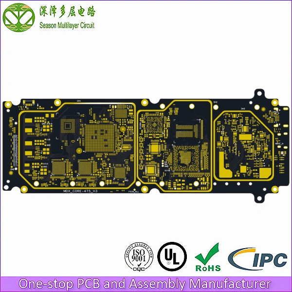
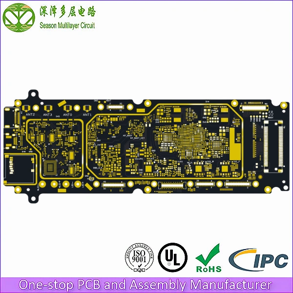
4+2+4
Any-Layer / ELIC Build
5/5
Adjacent Layer Pairs Laser-Connected
0.20 mm
Min Laser Microvia
2/2 mil
Inner Line / Space
OSP
Surface Finish
UL(305905)
IPC-A-600 Class 3
ISO 9001:2015
IATF 16949
RoHS / REACH
100% E-Test
What an Any-Layer HDI PCB Actually Is
In a 1-stage HDI board, one build-up layer per side carries laser microvias from the outer copper down to the first inner layer. A 2-stage board adds a second build-up layer per side. A 3-stage board adds a third. Any-layer HDI removes the stopping point altogether: every adjacent layer pair in the stack is joined by a laser microvia, so on a ten-layer board there are nine via pairs (L1-L2 through L9-L10) instead of the three to six pairs that 1-stage to 3-stage constructions provide. The acronym ELIC, for every layer interconnection, describes the same idea, and you will see both terms used for the same physical build.
The practical consequence is routing freedom. On a 2-stage board a signal entering at L4 and leaving at L6 has to travel through a through hole or find a landing layer inside the core. On an any-layer HDI PCB that signal simply steps L4 to L5 and L5 to L6 on laser microvias, which means fan-out can escape a fine-pitch BGA inward, not just outward. Ball fields sit above planes instead of above escape corridors, and the board gets thinner because every dielectric between the pairs can be held near the microvia diameter.
| Property | 1-stage / 2-stage / 3-stage HDI | Any-layer HDI (ELIC) |
|---|---|---|
| Laser via pairs on a 10-layer board | 2, 4 or 6 pairs, stopping at a buried-via core | 9 of 9 adjacent pairs, no stopping point |
| Signal path between arbitrary layers | Through a via that must reach a landing layer | Direct pair-to-pair steps anywhere in the stack |
| Dielectric thickness between pairs | Thin on the build-up, thicker inside the core | Thin everywhere: 59–64 µm between every pair |
| Lamination cycles (10 layers) | 2 to 4 after the core press | 4 after the core press, one per layer pair |
The stage ladder is set out in the HDI PCB technology guide, and a worked ten-layer 3-stage comparison lives in the 10-layer 3-stage HDI stackup review. The table below condenses the ladder to the decisions that matter when you are weighing any-layer HDI against the alternatives.
Any-Layer HDI PCB Versus a Standard Multilayer Board
A conventional ten-layer multilayer board routes everything through plated through holes. Each through hole consumes a keep-out on every layer it passes, which is why dense fine-pitch designs run out of channels long before they run out of layers. An any-layer HDI PCB spends its thin dielectrics on interconnect instead: the same ten layers carry more routing channels per square millimeter, the board is thinner, and every layer under a ball field stays available as a plane. The trade is process cost: each via pair is its own lamination, drilling and filling event, which is exactly why the build rules in the next sections exist.
The 10-Layer Any-Layer HDI Stackup
The reference build is symmetric around a single 0.064 mm core that carries L5 and L6 as foil-laminated core faces. Above and below it, four build-up layers per side are bonded with 1067 prepreg, and every one of the nine dielectrics stays between 59 and 64 µm so a 0.10 mm laser microvia keeps its 1:1 blind-via aspect ratio. Total finished thickness is 0.8 ± 0.10 mm including solder mask. This is the production stackup of the 10-layer any layer HDI PCB shown on this page; substitute dielectrics are listed under materials.
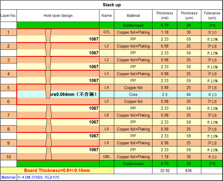
| Layer / band | Material | Thickness (µm) | Tolerance | Function in the any-layer HDI stack |
|---|---|---|---|---|
| Solder mask (top) | LPI solder mask ink | 20 | ≥ 5 µm | Pad definition over L1 lands |
| L1 (Top, GTL) | Copper foil + plating | 30 | ± 10 µm | Component-side signal layer; source of via pair V1 |
| Prepreg | 1067 glass fabric | 59 | ± 10% | Dielectric for V1 (L1–L2) |
| L2 (Inner) | Copper foil + plating | 25 | ≥ 18 µm | Landing pad for V1; signal and reference |
| Prepreg | 1067 glass fabric | 59 | ± 10% | Dielectric for V2 (L2–L3) |
| L3 (Inner) | Copper foil + plating | 25 | ≥ 18 µm | Signal layer; landing pad for V2 |
| Prepreg | 1067 glass fabric | 59 | ± 10% | Dielectric for V3 (L3–L4) |
| L4 (Inner) | Copper foil + plating | 25 | ≥ 18 µm | Signal layer; upper neighbour of the core |
| Prepreg | 1067 glass fabric | 59 | ± 10% | Bonds the L5 foil to the core package; dielectric for V4 (L4–L5) |
| L5 (Core face) | Copper foil, foil-laminated | 25 | ≥ 18 µm | Core-side signal and plane; landing pad for V4 |
| Core | FR-4 EM-370(D), Tg ≥ 170 °C | 64 | ± 10% | 0.064 mm laminate, copper excluded; carries V5 (L5–L6), drilled, filled and plated |
| L6 (Core face) | Copper foil, foil-laminated | 25 | ≥ 18 µm | Core-side signal and plane; source of V6 |
| Prepreg | 1067 glass fabric | 59 | ± 10% | Bonds the L6 foil outward; dielectric for V6 (L6–L7) |
| L7 (Inner) | Copper foil + plating | 25 | ≥ 18 µm | Signal layer; landing pad for V6 |
| Prepreg | 1067 glass fabric | 59 | ± 10% | Dielectric for V7 (L7–L8) |
| L8 (Inner) | Copper foil + plating | 25 | ≥ 18 µm | Signal layer; landing pad for V7 |
| Prepreg | 1067 glass fabric | 59 | ± 10% | Dielectric for V8 (L8–L9) |
| L9 (Inner) | Copper foil + plating | 25 | ≥ 18 µm | Signal layer; landing pad for V8 |
| Prepreg | 1067 glass fabric | 59 | ± 10% | Dielectric for V9 (L9–L10) |
| L10 (Bottom, GBL) | Copper foil + plating | 30 | ± 10 µm | Solder-side signal layer; source of V9 |
| Solder mask (bottom) | LPI solder mask ink | 20 | ≥ 5 µm | Pad definition over L10 lands |
Two details in this table carry most of the engineering weight. First, the copper weights are asymmetric on purpose: 30 µm on the outer faces for current handling and probe wear, 25 µm on the inner layers to keep etch geometry tight at 2/2 mil. Second, the dielectric ladder is uniform by design: all eight prepreg bands are 1067 glass at 59 µm, so every microvia pair sees identical laser, desmear and plating behavior, and the impedance model tracks a single Dk between reference planes.
Every Dielectric Is a Microvia Dielectric
On a 2-stage or 3-stage board, only the build-up dielectrics need to be laser-drillable; the core can be as thick as the impedance budget likes. On an any-layer HDI PCB the core is just another via pair, so the 0.064 mm laminate is chosen with the same discipline as the prepregs. That constraint is also what keeps the whole board thin: nine dielectrics at 59–64 µm plus ten copper bands come to a nominal 0.8 mm finished thickness inside a 0.8 ± 0.10 mm specification window, and heavier outer copper can be added without touching the laser microvia budget.
How the Any-Layer HDI Build Is Sequenced
An any-layer HDI PCB is a sequential lamination product: the board does not exist as ten layers until the last press, and each cycle adds one copper layer per side. The 0.064 mm core is the starting point. Its inter-pair via V5 is laser-drilled through the 64 µm laminate, filled with copper, plated and planarized before anything is laminated over it, so the core pair is complete before the first build-up cycle. From there, each cycle bonds one layer per side and closes two more via pairs.
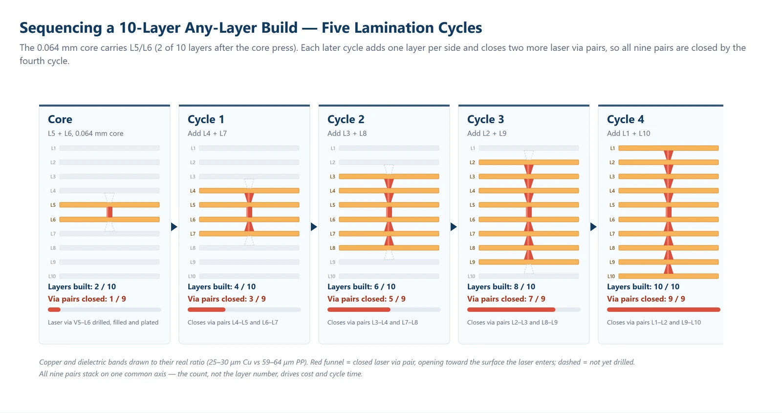
On an any-layer HDI PCB the cycle count is the cost model and the risk model at the same time. Each cycle is a separate yield, alignment and registration event, which is why any-layer HDI is quoted per build rather than per layer. It is also why defects are caught early: the core pair is electrically tested before the first build-up is laminated over it, and each later cycle can be X-ray checked against the alignment budget before the next press starts.
| Cycle | Layers added | Cumulative layers | Via pairs closed in this cycle |
|---|---|---|---|
| Core press | L5 + L6 (0.064 mm core) | 2 | V5 (L5–L6) — drilled, filled and plated in the core |
| Cycle 1 | L4 + L7 | 4 | V4 (L4–L5) and V6 (L6–L7) |
| Cycle 2 | L3 + L8 | 6 | V3 (L3–L4) and V7 (L7–L8) |
| Cycle 3 | L2 + L9 | 8 | V2 (L2–L3) and V8 (L8–L9) |
| Cycle 4 | L1 + L10 | 10 | V1 (L1–L2) and V9 (L9–L10) |
Any-Layer HDI Capability Envelope
The numbers below are the standing capability limits of our any-layer HDI PCB line, quoted the same way for any-layer builds as for 1-stage to 3-stage. Production values are what we hold on repeat orders; sample values are what we accept on prototype and small-volume runs where the extra process attention is affordable. If a requirement falls outside the production column, the DFM review will say so in writing before anything is scheduled.
| Parameter | Mass production | Sample runs |
|---|---|---|
| Layer count | 2 to 30 layers | 2 to 64 layers |
| Maximum HDI stages | 4+N+4 (up to four build-up layers per side) | Any-layer interconnect |
| Microvia diameter (minimum) | 4 mil (0.10 mm) | 3 mil (0.076 mm) |
| Mechanical drill (minimum) | 6 mil (0.15 mm) | 5 mil (0.127 mm) |
| Blind via aspect ratio | 1:1 | 1:1.2 |
| Through-hole aspect ratio | 12:1 | 20:1 |
| Inner layer line and space (minimum) | 2/2 mil | 1.8/1.8 mil |
| Outer layer line and space (minimum) | 2.5/2.5 mil | 2/2 mil |
| BGA pad (minimum) | 8 mil (0.20 mm) | 7 mil (0.18 mm) |
| Via to inner-layer trace (minimum) | 6 mil (0.15 mm) | 5 mil (0.127 mm) |
| Layer-to-layer alignment | 3 mil (0.076 mm) | 2 mil (0.05 mm) |
| Impedance tolerance | ±8% | ±5% |
| Finished thickness | 0.2 to 6.0 mm | 0.15 to 20 mm |
| Copper weight | 1/3 oz to 6 oz | 1/4 oz to 12 oz |
Key Advantages of This 10-Layer Any-Layer HDI PCB
- Nine laser via pairs on one common axis — a signal steps L1 to L10 across the any-layer HDI PCB stack without a single through hole. That is the defining ELIC PCB advantage: fan-out escapes a fine-pitch BGA inward over planes instead of outward through dogbone keep-outs.
- Every dielectric is a microvia dielectric — the 0.064 mm core is drilled, filled and plated like a build-up band, so every pair in this every layer interconnection PCB build holds a 1:1 blind-via aspect ratio and nothing in the stack blocks a laser via.
- 0.8 mm finished thickness for height-critical carriers — nine thin dielectrics and ten copper bands sum to a 0.8 mm any-layer HDI PCB, which is what camera modules, sensor carriers and wearable stacks actually budget for.
- Impedance re-tuned per dielectric band — the 59–64 µm ladder sits between reference planes, so every controlled net is mapped to its plane pair and re-tuned, then verified on a TDR coupon to ±8% in production and ±5% on sample runs.
- Defects escape early, not at final test — the core pair is electrically tested before the first build-up goes over it, and every later cycle is X-ray checked against the alignment budget before the next press, so an any-layer HDI PCB problem is caught at the cycle that caused it.
- One stackup from prototype to volume — the first any-layer HDI prototype build fixes the lamination profile, prepreg lots and impedance model that volume orders inherit, so a design qualified on samples does not change when it scales.
Overcoming Critical Challenges in Any-Layer HDI Production
1. Registration Across Nine Via Pairs
Nine stacked pairs concentrate the layer-to-layer alignment budget in the middle of the stack. We hold 3 mil (0.076 mm) at production, review annular rings pair by pair, and X-ray each chain crossing before the next lamination cycle is scheduled.
2. Via-in-Pad Fill on Every Landing Pad
In an any-layer HDI PCB every inner landing pad is a candidate via-in-pad. Fill-and-cap is applied where the BGA field needs it, verified by microsection on each lot, and planarity is checked before the next stage lands.
3. Cost Discipline: Convert When the Stack Allows
Full ELIC PCB pricing is a drill, fill and press event per pair. When only part of the stack truly needs laser connections, the DFM review quotes a cross blind-and-buried alternative side by side so the cost decision stays with your program.
4. Warpage Control on a Thin 0.8 mm Stack
Ten copper bands and nine dielectrics in one thin panel is a pressing challenge. The ladder is symmetric about the core, copper weights mirror top to bottom, and bow and twist are checked after final lamination on every lot.
Design Rules That Decide Whether an Any-Layer HDI PCB Works
Most any-layer HDI PCB programs succeed or fail on three decisions taken before the first Gerber is sent: where filled vias are really needed, how the alignment budget is spent, and how copper weight interacts with the 2/2 mil inner geometry. The three subsections below are the review list our CAM team walks through on every any-layer enquiry.
Via-in-Pad and Fill Geometry
On an any-layer HDI PCB a stacked microvia chain is only as strong as its first link: the stage-1 via must be filled and planarized before the next stage lands on it. In an any-layer HDI PCB every inner landing pad is a candidate via-in-pad, so fills are applied where the BGA field actually needs them rather than across the whole board. Fill quality is verified by microsection on each lot, and the planarity requirement is why we ask for the ball pitch map early: it decides how much of the stack is fill-and-cap and how much is plain laser via.
The Alignment Budget Across Nine Via Pairs
Nine via pairs on an any-layer HDI PCB mean nine chances for layer-to-layer misalignment, and the budget is 3 mil (0.076 mm) at production. Any-layer HDI concentrates that budget in the middle of the board where the microvia chains run, so annular ring sizes on inner layers are reviewed pair by pair rather than assumed. Where a chain crosses the core, the pair is X-ray checked against the budget before the next lamination; where a design calls for 2 mil alignment (sample runs), we review the chain positions against panel location before quoting.
Copper, Trace Width and Impedance
Inner layers run 2/2 mil line and space at production, with 25 µm copper; the outer faces run 2.5/2.5 mil at 30 µm. Impedance is controlled against the stated differential and single-ended targets on a TDR coupon, held to ±8% in production and ±5% on sample runs. Because the dielectric ladder alternates 60 and 96 µm bands, impedance references jump between adjacent layers, so the review maps every controlled-impedance net to its reference plane pair and re-tunes trace widths per band, instead of assuming one geometry everywhere.
Any-Layer HDI vs 3-Stage vs Cross Blind-and-Buried
The same ten layers can be built three ways, and the honest answer is that most designs asking for any-layer HDI only need part of the stack to be laser-connected. The comparison below sets out where the extra cycles of a full ELIC build pay for themselves and where they do not.

| Construction | Laser via pairs | Stack character | Cost direction | Best when |
|---|---|---|---|---|
| Any-layer (ELIC) | 9 of 9 pairs | Single 0.064 mm core, every dielectric 59–64 µm | Highest: a drill, fill and press event per pair | Most of the board needs laser connections between arbitrary layers |
| 3-stage HDI | 6 of 9 pairs | Four-layer core carries L4-L7; build-up on both faces | High: three build-up cycles per side | Dense outer fan-out over a planar core |
| Cross blind-and-buried | 4 of 9 pairs + buried pair | Thicker core with buried-via pairs | Lowest of the three | Only part of the stack is dense |
The economics of that last row are spelled out in the blind and buried via HDI guide, which documents reviewed conversions from any-layer intent to cross constructions: fewer drilling passes, less build-up dielectric and a shorter manufacturing chain. Where the opposite is true and the routing genuinely spans the stack, any-layer HDI remains the correct answer, and quoting the alternative alongside it is part of our DFM review either way.
Dielectrics and Laminate Options for Any-Layer HDI
Every dielectric in an any-layer HDI PCB stack doubles as a microvia dielectric, so material selection is constrained twice: the dielectric must laser-drill cleanly at 0.10 mm, and it must bond at the press temperatures of the cycles around it. The default stack uses 1067 prepreg over a 0.064 mm EM-370(D) FR-4 core at Tg ≥ 170 °C. The same ladder runs on the material classes below, with the impedance model re-tuned on the new Dk.
| Laminate class | Typical grades | Fit in an any-layer HDI stack |
|---|---|---|
| Standard FR-4, Tg ≥ 170 °C | EM-370(D) (default for this build) | Holds the 59–64 µm dielectric ladder with margin for lead-free reflow |
| Mid-loss FR-4 | TU-872 SLK | For longer high-speed channels; laser and press behavior comparable to the default |
| Low-loss FR-4 | IT-180A, MEGTRON 6 | For multi-gigabit nets; dielectric ladder re-validated at the DFM review |
| Halogen-free FR-4 | S1150G (Tg 150) | For environmental programs; thinner-band geometry reviewed case by case |
Full material data sheets and glass-weave behavior are covered on the PCB materials and laminates page. For an every layer interconnection PCB the practical rule is that a material must exist in thin, laser-drillable forms across the whole ladder; a high-performance core with no thin prepreg companion cannot serve a build where the core is just another via pair.
Where Any-Layer HDI Earns Its Cost
- Wearable and camera-module carriers where every 0.1 mm of height is budgeted and the processor fan-out must escape inward over planes
- Edge-computing and industrial control boards with dense fine-pitch processors and little room for through-hole keep-outs
- Automotive cockpit sensing modules that concentrate cameras and radar-side processing on one thin carrier
- Handheld diagnostic and lab-instrument devices where probe-side electronics must sit inside a small, sealed enclosure
- Substrate-like routing density in conventional PCB form, when a true package substrate is not justified at the volumes involved
If the board is an SoM or compute module rather than a single-function carrier, the same interconnect logic is documented from the module angle on the 12-layer 2-stage HDI core board page, and the automotive cockpit variant of that build is on the 12-layer 2-stage HDI automotive PCB page.
Inspection and Reliability Checkpoints
Every laser via pair in an any-layer HDI PCB is a separate drilling, filling and plating event, so verification on the any-layer HDI PCB is structured per pair rather than per board. Outer-layer imaging runs through AOI on both faces; X-ray reads layer-to-layer registration against the 3 mil budget at the core crossings; microsections through the stacked via chains verify fill, plating and planarity on every lot; TDR coupons confirm impedance against the stated targets; and flying-probe or fixture test closes every net across all nine pairs.
The records travel with the panel: impedance coupon results, the microsection images, the X-ray registration reading and the electrical test file are filed per lot, so an assembly question months later can be traced back to the exact build that produced the board. Workmanship follows IPC standards.
From Any-Layer HDI Prototype to Volume
The first build fixes the parameters that later orders inherit: the lamination profile, the prepreg lots, the impedance model and the alignment budget. Prototypes are run with sample-run tolerances (0.076 mm microvias, ±5% impedance, 2 mil alignment) where the design needs them, and the DFM review flags every parameter that would tighten for production so the transition holds no surprises.
Volume orders run the same stackup on the production envelope (0.10 mm microvias, ±8% impedance, 2/2 mil inner geometry), with the per-lot inspection package unchanged. Panelization is engineered against your Gerber so utilization survives the stricter production window, and engineering review confirms the lead time for each batch before scheduling. Gerber data is accepted as Gerber RS-274X or ODB++.
Why Season PCB for Any-Layer HDI
- Group manufacturing since 2006 across three plants (Shenzhen, Jiangxi, Anhui) with 3,000,000 m² of annual capacity; the ELIC PCB line is part of the same quality system as the multilayer backbone
- 2 to 30 layers in production, 1-stage through any-layer HDI, with sample runs to 64 layers
- 0.10 mm laser microvias as the production default, 0.076 mm on sample runs, with fill and planarization verified by microsection per lot
- Certified systems: IPC workmanship, UL (E305905), ISO 9001, IATF 16949 and RoHS compliance
- Turnkey assembly available: the same group runs SMT and PCBA, so the any-layer carrier can be quoted populated
- Written DFM feedback on every enquiry, including the cross blind-and-buried alternative when the stack does not need full ELIC
Group background and capacity data are on the 998 PCB Group overview, and the full HDI product range is in the HDI PCB category.
Frequently Asked Questions
What does any-layer HDI (ELIC) actually mean?
Any-layer HDI means every adjacent layer pair in the stack is connected by a laser microvia, with no stopping core for the interconnect. On a ten-layer board that is nine via pairs, L1-L2 through L9-L10. ELIC stands for every layer interconnection and names the same construction; some laminate vendors market the process under proprietary names, but the generic terms any-layer HDI and ELIC PCB describe the same build.
How is an any-layer HDI PCB different from a 3-stage HDI build?
A 3-stage board has three build-up layers per side over a buried-via core, so its laser vias stop at the core faces, so on a ten-layer build that is six via pairs instead of nine. Inside the core, connections travel on core routing and buried vias. The worked comparison is in the 10-layer 3-stage HDI stackup review; the short version is that 3-stage is the right answer when the dense fan-out lives on the outer layers and the core can stay planar.
When is any-layer worth the extra lamination cycles?
When most of the board genuinely needs laser connections between arbitrary layer pairs: dense fan-out on inner layers, signals stepping across the whole stack, or a height budget that rules out through holes. If the any-layer request is driven by part of the stack rather than all of it, a cross blind-and-buried construction usually recovers both cost and lead time, and our DFM review quotes the alternative alongside the full ELIC build so you can compare.
What layer counts and thicknesses can an any-layer HDI PCB use?
An any layer HDI PCB can be built from 2 to 30 layers in production and to 64 layers on sample runs. The ten-layer reference build on this page finishes at 0.8 mm with nine via pairs; thinner and thicker boards scale with the dielectric ladder. Production microvias are 0.10 mm with a 1:1 blind-via aspect ratio, and sample runs accept 0.076 mm.
Which dielectrics work in an any-layer HDI stack?
Every dielectric in an every layer interconnection PCB must be laser-drillable at the production microvia diameter, so the ladder is built from thin 1067 prepreg (59-micron plies in the reference build) over a 0.064 mm EM-370(D) FR-4 core at Tg 170 or above. Mid-loss and low-loss grades such as TU-872 SLK, EM-370(Z), IT-180A and MEGTRON 6 run the same ladder with the impedance model re-tuned; halogen-free programs use S1150G.
How are the nine via pairs verified on your line?
Per pair, not per board. AOI reads both outer faces, X-ray checks layer-to-layer registration against the alignment budget, microsections through the stacked via chains verify fill, plating and planarity on every lot, TDR coupons confirm impedance, and flying-probe or fixture test closes every net. The records ship with the panel, so the data behind each any-layer HDI PCB stays traceable.
What files do you need to quote an any-layer HDI PCB?
Gerber RS-274X or ODB++ data for the any-layer HDI PCB, the target stackup or finished thickness, impedance targets with their nets, the BGA pitch map, surface finish and the mechanical outline. If the stackup is not fixed yet we propose one from the ball pitch and layer count, and the DFM feedback comes back in writing with the quotation.
Can an any-layer design be converted to a cheaper structure?
Often, yes. The review maps which nets actually need laser connections between arbitrary layers; when that is a subset of the stack, a cross blind-and-buried build delivers the same interconnect plan as the ELIC PCB with fewer drilling passes and less build-up dielectric. Conversions are quoted side by side with the any-layer HDI build on cost, lead time and risk, and the choice stays with your program.
Ready to Start Your Any-Layer HDI Project?
Send the Gerber data, the target stackup and the impedance targets, and we will return a written DFM review, including the cross blind-and-buried alternative if the stack does not need full any-layer interconnect. You will know which structure fits before the first panel is scheduled.