Skip to content
  • Home
  • Services
  • Products
    • Fast PCB
    • Multilayer PCB
    • HDI PCB
    • High Speed PCB
    • High Frequency PCB
    • Rigid-Flex PCB
    • PCBA
  • Instant PCB Quote
  • About Us
    • Company Profile
    • Factory Display
    • Process Capability
    • Lead Time
    • HDI PCB Technology
    • PCB Materials and Laminates
  • News
  • Contact

Book Appointment Now

(+86) 1868152853224/7 Emergency Phone
Season PCB logo - PCB manufacturer in Shenzhen, China
  • Home
  • Services
  • Products
    • Fast PCB
    • Multilayer PCB
    • HDI PCB
    • High Speed PCB
    • High Frequency PCB
    • Rigid-Flex PCB
    • PCBA
  • Instant PCB Quote
  • About Us
    • Company Profile
    • Factory Display
    • Process Capability
    • Lead Time
    • HDI PCB Technology
    • PCB Materials and Laminates
  • News
  • Contact
(+86) 1868152853224/7 Emergency Phone
Season PCB logo - PCB manufacturer in Shenzhen, China

Materials & Surface Finishes

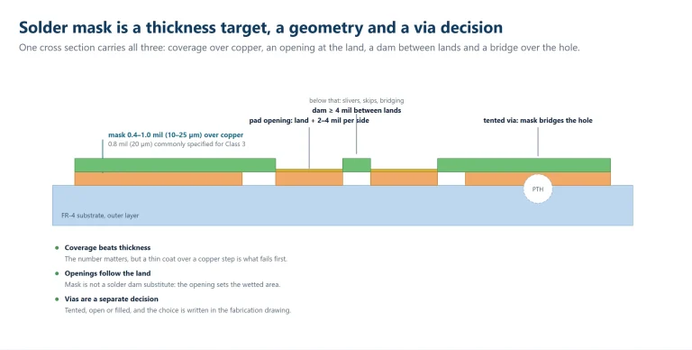
Solder mask selection cross section showing mask thickness over copper, a land opening, the dam between lands and a tented via

PCB Solder Mask Selection: Ink, Thickness and CTI Checks

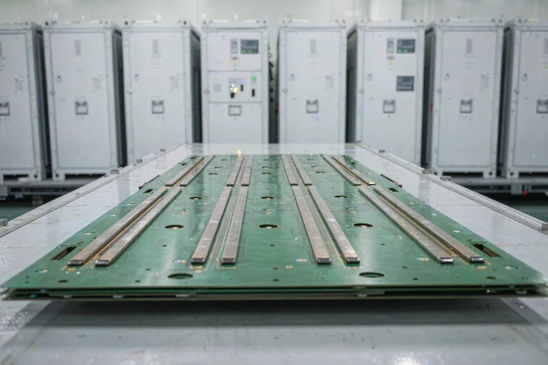
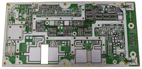
Large multilayer energy storage PCB panel on a production table in front of battery cabinets

Energy Storage PCB: Heavy Copper, Materials and Supplier Audit

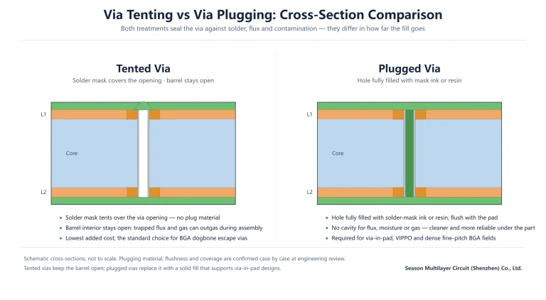
Via tenting vs via plugging cross-section: a tented via covered by solder mask and a plugged via fully filled with ink

Via Tenting vs Via Plugging: How to Choose the Right Via Finish

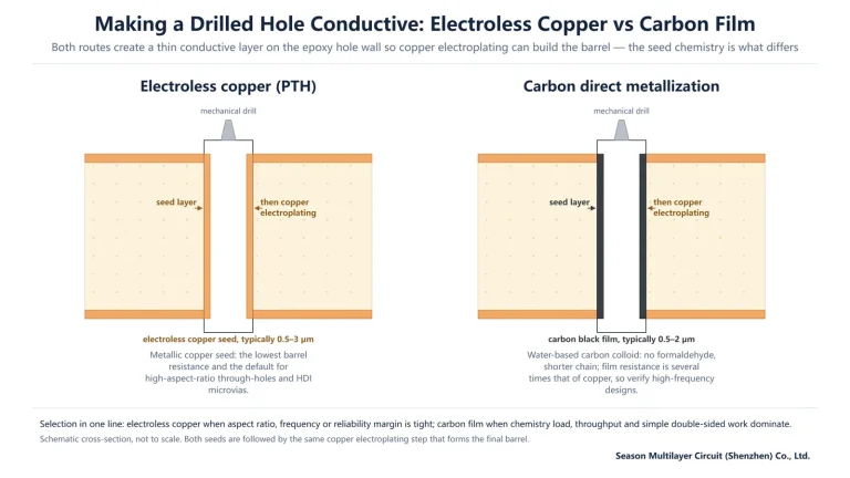
Black hole vs electroless copper cross-section comparison: electroless copper seed versus carbon black direct metallization on a drilled hole wall

Black Hole vs Electroless Copper: PCB Hole Metallization Compared

PCB Via Plugging: Resin Plugging vs Solder Mask Ink Plugging

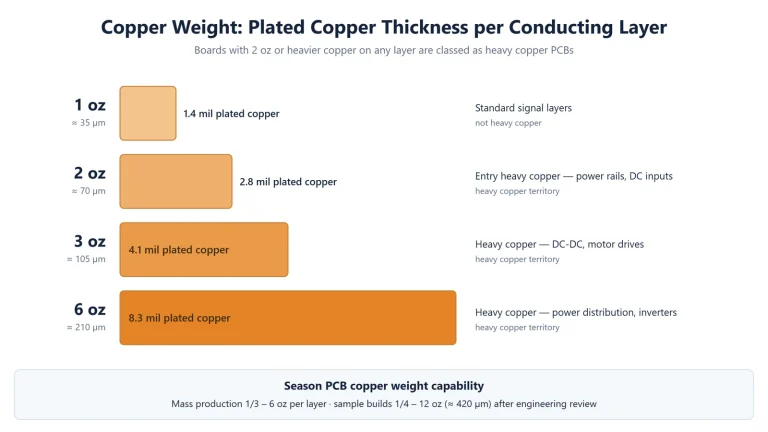
Copper weight ladder showing plated copper thickness for 1 oz, 2 oz, 3 oz and 6 oz heavy copper PCB layers with mass production and sample build capability

Heavy Copper PCB: Copper Weight, Current Capacity and When to Spec It

High-Frequency PCB: Materials, Dk/Df and When to Spec Them

Electroless Copper Deposition in PCB: How the PTH Process Works

ENEPIG Surface Finish: Pros, Cons and When to Specify It

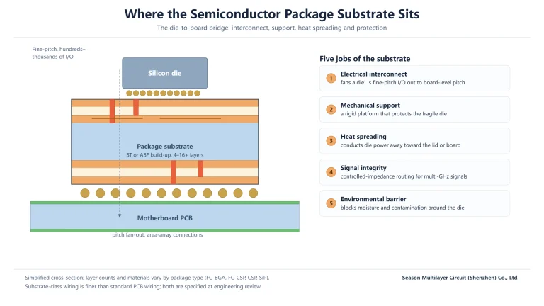
Cross-section showing a silicon die, flip-chip bumps, the package substrate and BGA balls connecting to a motherboard PCB

Semiconductor Package Substrate Explained: Functions, Materials and Types

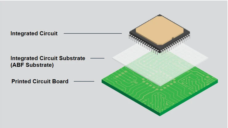
ABF Substrate Explained: Build-Up Film, Fine Lines and FC-BGA

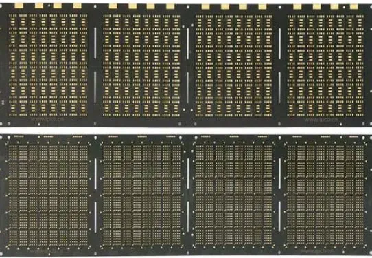
BT Substrate Explained: Properties, Applications and Selection

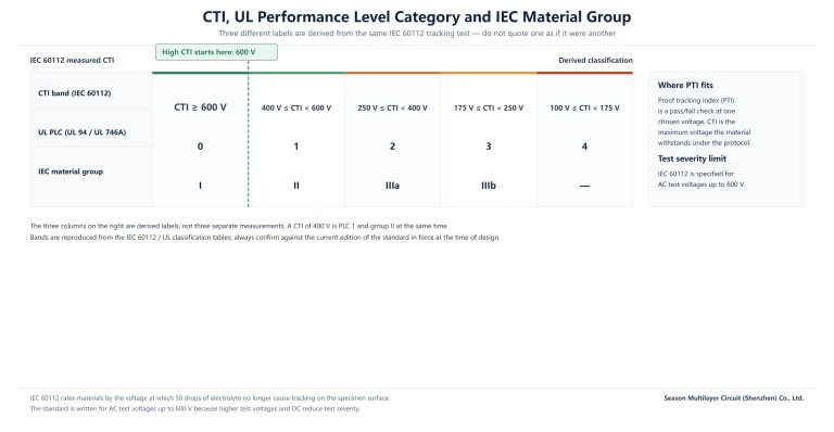
Table relating IEC 60112 CTI voltage bands to UL performance level categories and IEC material groups, with the 600 V high CTI threshold marked

High CTI PCB Explained: Ratings, Creepage Rules and Material Choice
About Us
We are a professional manufacturer specialized in HDI and multilayer PCBs, focusing on advanced manufacturing processes for high-end HDI, multilayer PCBs, flexible printed circuits (FPCs), and rigid-flex boards, along with comprehensive services including SMT processing and PCBA OEM/ODM solutions with material procurement.
Main Products
HDI PCB
Fast PCB Sample
Multilayer PCB
High Frequency PCB
High Speed PCB
Rigid-Flex PCB
PCBA turnkey service
Resources
PCB Basics
HDI & Microvias
Stackup & Impedance
Materials & Surface Finishes
Manufacturing Process
Assembly & Test
Standards & Certification
Industry News
Address
7F, Block A, Junfeng Business Building, 176 Chongqing Road, Fuhai Street, Baoan District, Shenzhen 518103
Tel: +86 18681528532
E-mail: roc@season-pcb.com

Copyright © 2006-2026 Season Multilayer Circuit (Shenzhen) Co., Ltd.