Book Appointment Now

Double-sided Rogers High-Frequency PCB
Double-sided Rogers high-frequency PCB built on RO4350B with stable Dk 3.48 and low Df 0.0037 at 10 GHz – engineered for base stations, radar front-ends and aerospace RF links, shipped from fast-turn prototype to small-batch production by Season PCB.
RO4350B combines PTFE-level electrical performance with standard FR-4 manufacturability: it drills, plates and etches on conventional PCB equipment, keeping lead times short and yields high for double-sided RF prototypes. The 1.6 mm symmetric stack pairs 35 μm (1 OZ) copper on both faces with 12/12 mil line/space resolution and 2 μin immersion gold ENIG pads, so a 50 Ω microstrip behaves identically from the first board to the thousandth.
- RO4350B hydrocarbon ceramic laminate – PTFE-level performance with FR-4 processability
- Dk 3.48 ± 0.05 / Df 0.0037 at 10 GHz for predictable impedance and tight loss budgets
- 1.6 mm double-sided stack with 35 μm copper, 0.4 mm minimum PTH and ENIG finish
- Tg > 280 °C and IPC Class 3 acceptance for lead-free reflow and high-reliability RF builds
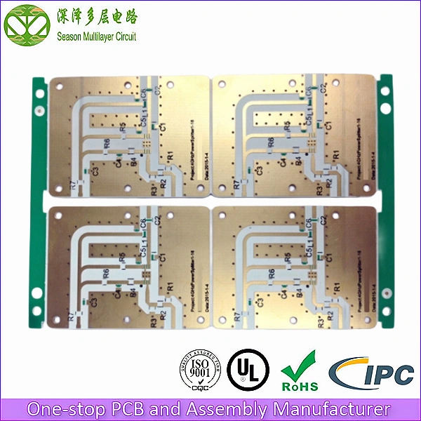
2-Layer
Rogers RO4350B
1.6 mm
Board Thickness
35 um Cu
Both Sides
0.4 mm
Min PTH
Dk 3.48
Stable @10 GHz
UL Listed
IPC-A-600 Class 3
ISO 9001:2015
IATF 16949
RoHS / REACH
100% E-Test
Double-sided Rogers High-Frequency PCB Stackup Diagram
RO4350B Double-Sided Stackup (1.6 mm total, 35 μm Cu both sides, ENIG)
- L1 (Top Copper) – 35 um Electrodeposited: L1 (Top Layer) — 35 μm electrodeposited copper, used for microstrip RF traces, patch antennas, component pads and SMD solder lands.
- RO4350B Hydrocarbon Ceramic Core – 1.53 mm: RO4350B Hydrocarbon Ceramic Core — 1.53 mm nominal thickness, Dk 3.48 ± 0.05, Df 0.0037 at 10 GHz, Tg > 280 °C, tightly controlled dielectric for repeatable impedance.
- L2 (Bottom Copper) – 35 um Electrodeposited: L2 (Bottom Layer) — 35 μm electrodeposited copper, used for RF ground pours, DC power distribution, bias networks and stitching via arrays.
- Symmetric 1+0+1 Single-Core Lamination Cycle: 35 μm Copper on Both Faces — symmetric 1 OZ outer layers maintain mechanical balance, prevent warpage during reflow and simplify impedance modelling.
- 0.4 mm Plated Through-Holes Spanning L1 to L2: Plated Through-Holes ≥ 0.4 mm — mechanically drilled, electroless + pattern plated; carry RF, DC and thermal current between L1 microstrip and L2 ground.
- ENIG 2 u” Immersion Gold Finish on Outer Pads: ENIG 2μ” Surface Finish — immersion gold over electroless nickel; flat, oxidation-resistant, wire-bondable and lead-free reflow compatible.
- 1.6 mm Finished Thickness for Sub-6 GHz Designs: Symmetric 1+0+1 Construction — single-core lamination cycle, shortest possible signal return path and lowest parasitic stub.
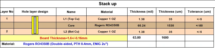
This 2-layer double-sided Rogers RO4350B stackup is a production-proven reference for wireless base-station power amplifiers, radar front-ends, satellite RF links and medical electronics. Our RF engineering team tunes the laminate grade (RO4350B / RO4003C / RO4450F), copper weight, and dielectric thickness to your impedance target and insertion-loss budget – all on a single sequential build-up for the shortest possible lead time on double-sided Rogers prototypes and production.
Technical Capability & Specifications
| Parameter | Specification |
|---|---|
| Layer Count | 2 layers (double-sided) |
| Base Material | Rogers RO4350B (hydrocarbon ceramic, glass-reinforced) |
| Finished Thickness | 1.6 mm ± 0.16 mm |
| Panel Size | 132 × 86 mm (4-up production panel) |
| Outer Layer Copper | 35 µm (1 OZ) on both sides |
| Minimum Plated Through-Hole | 0.4 mm |
| Blind / Buried Via | Not applicable (single-core construction) |
| Line / Space | 12 / 12 mil (305 µm) |
| Impedance Control | 50 Ω single-ended, 90 Ω differential, TDR-verified |
| Surface Finish | ENIG 2 µ” (immersion gold over electroless nickel) |
| Solder Mask | Green / blue / black / red LPI, optional peelable mask |
| Legend (Silkscreen) | White / yellow, top side or both sides |
| Operating Temperature | −55 °C to +150 °C continuous (Tg > 280 °C) |
| Lead-Free Reflow | Compatible, peak 260 °C, 6× cycles verified |
| Dielectric Constant (Dk) | 3.48 ± 0.05 @ 10 GHz (RO4350B) |
| Dissipation Factor (Df) | 0.0037 @ 10 GHz (RO4350B) |
| Acceptance Standard | IPC-6012 Class 3, IPC-A-600 |
| Quality System | ISO 9001:2015, UL 796, RoHS / REACH compliant |
Key Advantages of Our Double-sided Rogers High-Frequency PCB
- Genuine Rogers RO4350B Hydrocarbon Ceramic Laminate: Stable Dk 3.48 ± 0.05 at 10 GHz: RO4350B holds its dielectric constant flat across frequency and temperature, so the 50 Ω microstrip you designed in the simulator is the 50 Ω microstrip you measure on the bench. No re-spins for impedance drift.
- Dk 3.48 +/- 0.05 at 10 GHz for Predictable Impedance: Low Df 0.0037 for Sharper Filters: with a dissipation factor an order of magnitude lower than FR-4, RO4350B reduces insertion loss in microstrip filters, diplexers and matching networks, helping you hit your link budget without extra LNA stages.
- Low Df 0.0037 to Cut Insertion Loss in RF Filters: FR-4-Compatible Processing: unlike pure PTFE, RO4350B can be drilled, plated and etched with standard PCB equipment, which means 5–7 day lead times for prototypes and stable yields for 50–500 piece production runs.
- FR-4-Compatible Drilling and Plating Process: Lead-Free Reflow Ready: Tg > 280 °C and CTE matched to copper give RO4350B double-sided boards the thermal headroom to survive lead-free reflow profiles up to 260 °C without delamination or barrel cracking.
- Lead-Free Reflow Compatible, Tg > 280 degree C: ENIG 2μ” for Flat RF Pads: immersion gold over electroless nickel produces an exceptionally flat pad surface, ideal for fine-pitch QFN RF ICs, SMT antennas and wire bonding, while keeping the surface oxidation-free during long storage.
- ENIG 2 u” Flat Pad Finish for SMT / Wire Bond: 100 % E-Tested and Impedance-Controlled: every double-sided Rogers panel is 100 % net-list tested, AOI inspected, and impedance cross-checked with a TDR coupon — production samples ship with measured impedance data you can file into your quality binder.
Overcoming Critical Challenges in Double-sided Rogers PCB Manufacturing
1. Continuous RF Ground on a Double-Sided Stack
How do you keep the RF ground continuous without blind or buried vias? We use dense plated through-hole via fences along the perimeter of every RF trace and a continuous L2 ground pour, stitching the L1 signal layer to the L2 ground at ≤ λ/20 spacing. Because RO4350B is single-core, every signal via reaches the ground plane in one short barrel, eliminating the parasitic stub of a stacked HDI via and keeping the return path compact at 6 GHz.
2. Drilling and Plating 0.4 mm PTH in RO4350B Ceramic
How do you avoid resin recession and rough hole walls in hydrocarbon ceramic cores? We use optimized drill parameters (peck drilling, new carbide bits, controlled infeed), plasma desmear before electroless copper, and high-temperature glycol-free electroless plating chemistry. The result is < 25 μm resin recession and a smooth hole wall that survives 6 × 260 °C lead-free reflow without barrel cracking.
3. Lead-Free Reflow Survival on Ceramic Cores
How do you prevent copper-epoxy delamination under lead-free reflow? Each RO4350B panel is baked at 150 °C for 4 hours before lamination to drive out absorbed moisture, and the lamination profile uses a slow ramp-up rate and extended cure stage above 200 °C. TMA (thermo-mechanical analysis) verifies Tg > 280 °C, and cross-sections confirm no delamination after 6 × reflow.
Where Our Double-sided Rogers High-Frequency PCBs Are Used
- Wireless Base-Station Power Amplifiers: Wireless Base-Station Power Amplifiers: 50 Ω microstrip RF traces, 90 Ω differential pair bias lines and isolated DC domains on a single RO4350B core, repeatable from prototype to mass production.
- Radar Front-End and LNA Modules: Radar Front-End and LNA Modules: low Df 0.0037 keeps NF figure low for automotive 77 GHz radar, FWCW altimeters and security mmWave sensors; controlled impedance keeps the chain matched to the antenna.
- Satellite and Aerospace RF Links: Satellite and Aerospace RF Links: RO4350B’s thermal stability, low outgassing and IPC Class 3 build quality suit LEO satellite receivers, down-converters, GNSS patch antennas and flight-control RF boards.
- Medical Electronics Imaging and Monitoring: Medical Electronics Imaging and Monitoring: predictable Dk and low loss keep ultrasound front-ends, MRI receive arrays and patient monitoring RF links quiet and matched; lead-free compatible for medical-grade assemblies.
- Test & Measurement and Instrumentation: Test & Measurement and Instrumentation: vector network analyzer fixtures, RF test jigs and laboratory-grade adapters that need flat return loss from DC to 6 GHz, hand-built on the same RO4350B core with measured impedance reports.
Our Quality Guarantee for Double-sided Rogers High-Frequency PCBs
Every double-sided Rogers high-frequency PCB is built to the same quality system that supplies aerospace and medical OEMs — not a one-off prototype line. Below is the manufacturing and inspection coverage you get with every order.
- Material lot traceability: each panel ships with a Rogers COC showing dielectric constant, dissipation factor and Tg of the actual RO4350B lot.
- Impedance control: 50 Ω single-ended and 90 Ω differential microstrip coupons cross-checked with Polar Si9000 stackup and TDR on every production lot.
- 100 % electrical test: flying-probe net-list verification against the original CAD data; opens and shorts are zero before lamination and again after ENIG.
- AOI and visual inspection: automated optical inspection on both sides plus 100 % visual on pad edges, drill entry and silkscreen; AOI rejects rework before it reaches reflow.
- Cross-section and microsection: periodic cross-section of plated through-holes, copper plating thickness, ENIG thickness and dielectric spacing — documented for customer audit.
- Solderability and reflow: lead-free reflow simulation up to 260 °C on every new lot; ionic cleanliness tested to IPC-TM-650 2.3.25 with < 1.56 μg/cm² NaCl equivalent.
- Quality system: ISO 9001:2015, ISO 14001:2015, UL 796 and IPC-A-600 Class 3 acceptance; full PPAP / IMDS / FAI documentation available on request.
Why Choose Season PCB for Your Double-sided Rogers High-Frequency PCB?
Season PCB is the in-house RF engineering partner you want behind your next double-sided Rogers PCB program. Every board is supported by free DFM review, in-house impedance modelling, and 20+ years of high-frequency laminate experience.
Here is what every double-sided Rogers board we ship is backed by:
- 20+ years of PCB manufacturing experience backed by 998PCB Group’s large-format facility in Shenzhen.
- Free DFM and stackup review by RF engineers before tooling — impedance modelling included at no charge.
- In-stock RO4350B, RO4003C, RO4450F, Taconic, Arlon, F4B and Isola laminates for fast-turn prototypes.
- In-house LDI direct imaging, plasma desmear, ENIG line and impedance TDR coupon testing.
- Production samples ship with measured impedance data and cross-section reports when requested.
- Global DDP shipping, batch traceability and lifetime quality archive for every shipped lot.
Season PCB specializes in double-sided Rogers high-frequency PCB manufacturing for wireless, radar, aerospace and medical-electronics front-end modules – from base-station power amplifiers to satellite RF links and laboratory instrumentation. Our double-sided Rogers RO4350B build-up features genuine Rogers hydrocarbon ceramic laminate, 1.6 mm symmetric core, 12/12 mil controlled-impedance routing, 0.4 mm plated through-holes, and ENIG 2 u” finish for flat, oxidation-free RF pads.
For your high-frequency project, Season PCB provides fast turnaround, competitive pricing, and ISO-certified quality. 998PCB Group, established in 2006, supports the same program from Rogers prototype to mass production across both English and Chinese channels.
Our double-sided Rogers boards are built to high-speed and high-frequency PCB manufacturing standards and can scale into high-layer-count PCB mass production, or be paired with one-stop PCBA assembly service covering RF module placement and module-level testing. Pair these Rogers boards with our broader High Frequency PCB product line for the rest of your microwave and RF projects.
Frequently Asked Questions
What is the lead time for double-sided Rogers RO4350B PCBs?
Standard lead time is 5–7 working days for prototypes and 7–10 working days for small-batch production. For 50 × 86 mm single-up boards, 1–2 day expedite is available on stock RO4350B cores.
Can Rogers RO4350B be combined with FR-4 for hybrid stack-ups?
Yes. RO4350B bonds well to FR-4 prepreg (such as 1080 or 2113) for hybrid 4-layer or 6-layer builds. The transition is impedance-modelled and verified with TDR; send your stackup and we will return a DFM report.
What surface finishes do you offer for high-frequency Rogers boards?
ENIG 2μ” is the default for RF pads because of its flatness and oxidation resistance. We also support immersion silver, immersion tin, OSP and HASL lead-free; ENEPIG is available for wire-bond and gold-finger applications.
What file formats do you accept for double-sided Rogers PCB orders?
We accept Gerber RS-274X (preferred), ODB++ (preferred for impedance modelling), and Altium / KiCad / PADS / Allegro / Eagle native files. We can also work from your stackup table and netlist if the CAD is under NDA.
Ready to start your double-sided Rogers high-frequency project?
To receive a formal quote for double-sided Rogers high-frequency boards, send your Gerber or ODB++ files, board outline (DXF preferred), target impedance, and operating frequency range. Whether you need 5 pieces for an RF lab prototype or 5,000 modules for an aerospace program, our engineering team responds within 24 hours with DFM feedback, a stackup drawing, and a quote.