Skip to content
Home
Services
Products
Fast PCB
Multilayer PCB
HDI PCB
High Speed PCB
High Frequency PCB
Rigid-Flex PCB
PCBA
Instant PCB Quote
About Us
Company Profile
Factory Display
Process Capability
Lead Time
HDI PCB Technology
PCB Materials and Laminates
News
Contact
Book Appointment Now
(+86) 18681528532
24/7 Emergency Phone
Home
Services
Products
Fast PCB
Multilayer PCB
HDI PCB
High Speed PCB
High Frequency PCB
Rigid-Flex PCB
PCBA
Instant PCB Quote
About Us
Company Profile
Factory Display
Process Capability
Lead Time
HDI PCB Technology
PCB Materials and Laminates
News
Contact
(+86) 18681528532
24/7 Emergency Phone
Menu
HDI & Microvias
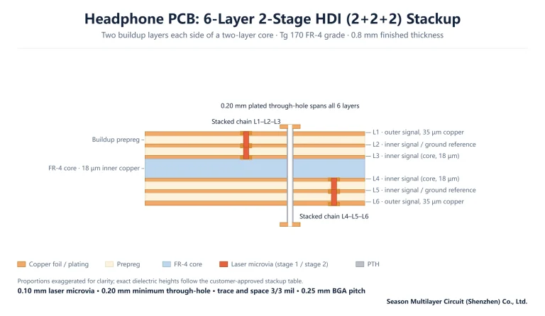
Headphone PCB: 6-Layer 2-Stage HDI for TWS and Audio Design
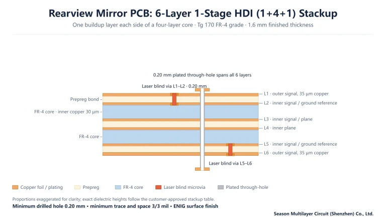
Rearview Mirror PCB: 6-Layer 1-Stage HDI Stackup and Specs
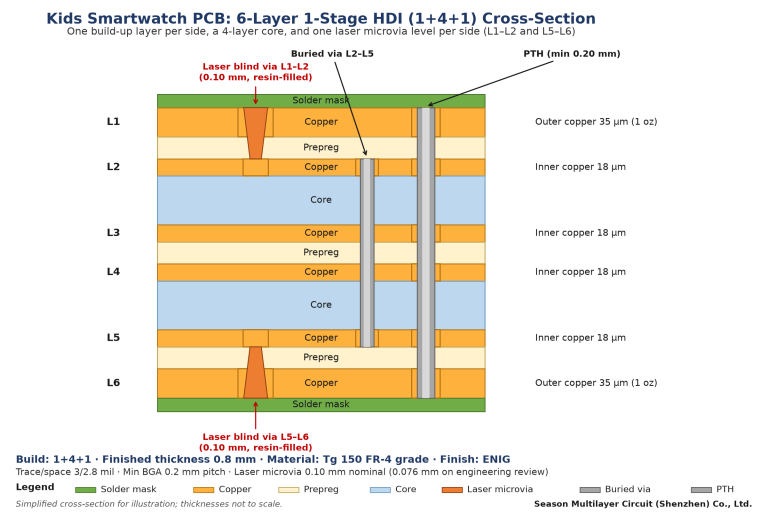
Kids Smartwatch PCB: Proven 6-Layer HDI Stackup and Specs
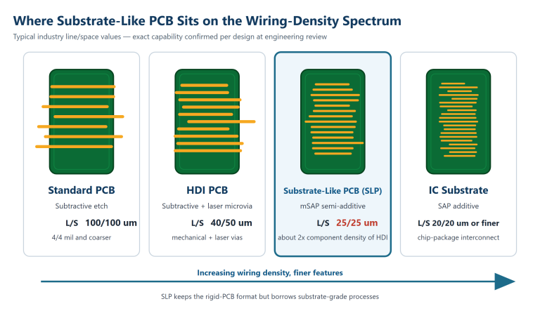
Substrate-Like PCB (SLP): mSAP Process, L/S Limits and 5 Proven Uses
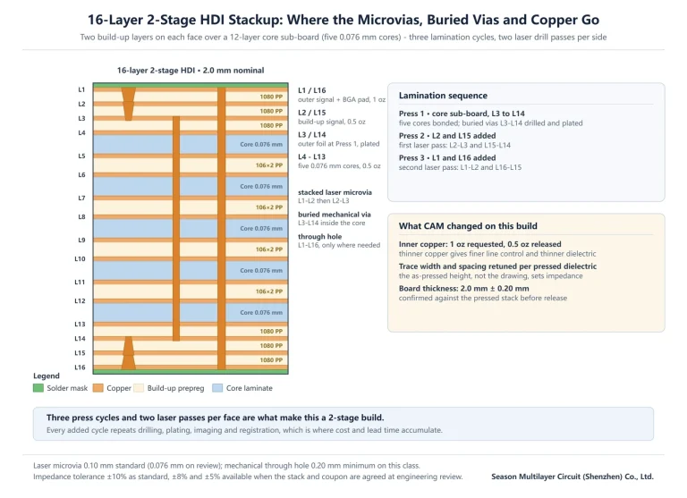
16-Layer 2-Stage HDI PCB: What a CAM Review Changes Before Production
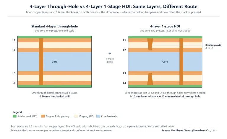
HDI PCB vs Standard PCB: 6 Best Stackup, Routing and Cost Answers
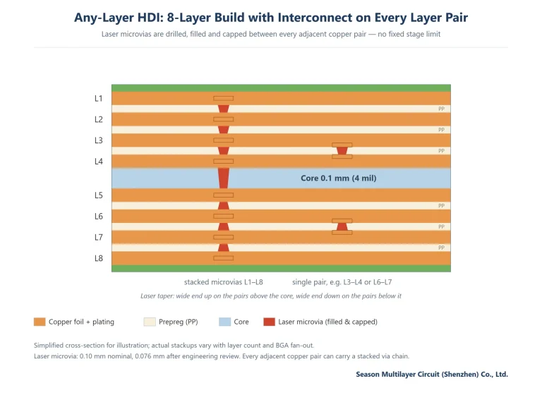
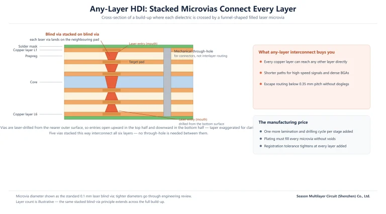
Any-Layer HDI Explained: ELIC Stackup, Process Flow and When to Use It
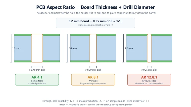
PCB Aspect Ratio Explained: Hole Size, Plating Throw and Design Limits
Via-in-Pad Technology for HDI and BGA Boards: Process and Rules
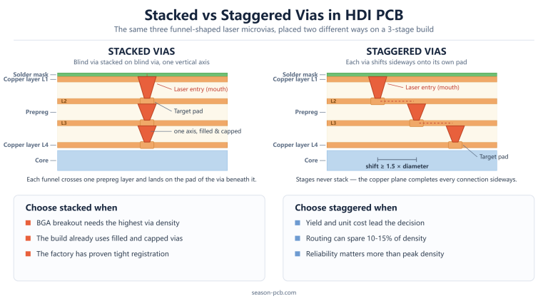
Stacked vs Staggered Vias in HDI PCB: Structures, Cost and Yield
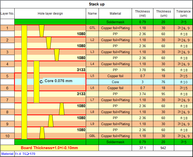
10-Layer 3-Stage HDI Stackup: Standard and Simplified Builds
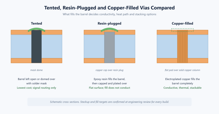
Copper Filled Vias: Via Filling Plating Process and Design Rules
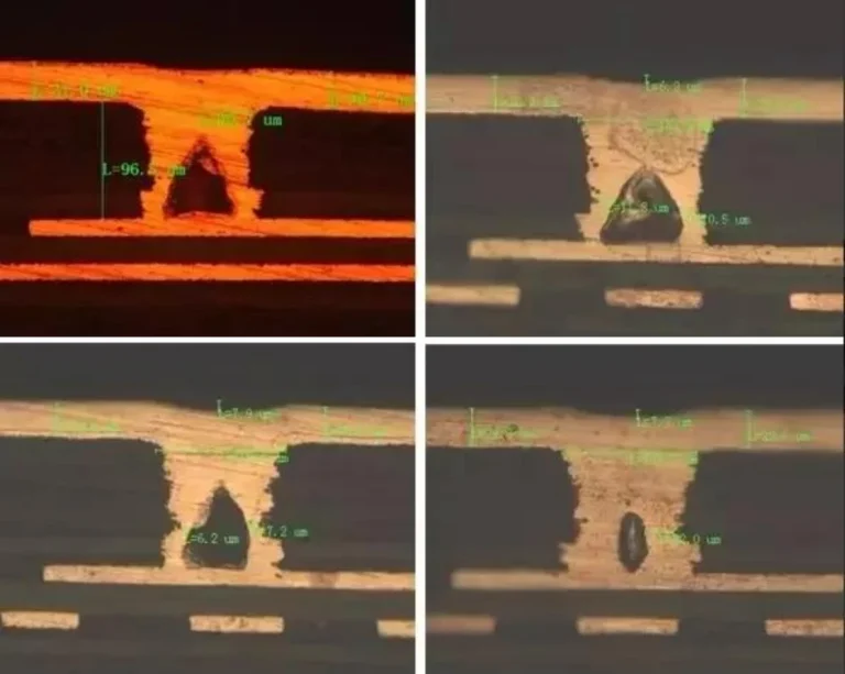
Plating Voids in Microvias: Root Causes and How Factories Fix Them
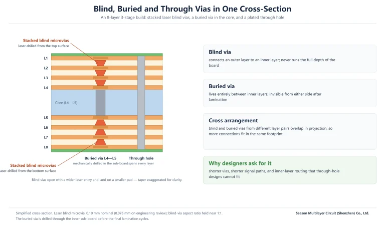
Blind and Buried Via HDI: Cross Via Structures for High-Density PCBs
Why Advanced HDI PCB Manufacturing Is Hard: Microvias, Yield and Cost
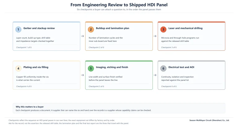
HDI PCB Manufacturer: How to Read a Factory’s Real Capability
HDI Stages Explained: 1-Stage, 2-Stage and 3-Stage PCB Stackups
998 PCB Group: Shenzhen HDI & Multilayer PCB Manufacturer
What is an HDI PCB