Book Appointment Now

How 1-stage, 2-stage and 3-stage HDI stages differ in stackup, laser drilling, cost and prototype lead time, plus a selection table by BGA pitch.
HDI Stages Explained: 1-Stage, 2-Stage and 3-Stage PCB Stackups

Most HDI quoting arguments come down to one question: how many HDI stages does this design actually need? Ask three people and you will usually get three answers, because “1-stage”, “2-stage” and “3-stage” describe lamination and laser-drilling work rather than a quality tier. A 3-stage board is not a better board; it is a board that needed three rounds of microvia formation to escape the routing it was given.
This article explains what counts as a stage, how HDI stages differ in stackup and process parameters, what each step does to cost and prototype lead time, and how to pick a stage from BGA pitch and layer count instead of from habit. It closes with the two specification mistakes that most often add cost without adding capability.
Table of Contents
- What Counts as a Stage in HDI PCB Manufacturing
- HDI Stages Explained: 1-Stage, 2-Stage and 3-Stage Build-Ups
- Process Parameters Compared Across HDI Stages
- How HDI Stages Change Cost
- Prototype Lead Time by HDI Stage
- Choosing Between HDI Stages by BGA Pitch and Layer Count
- Stacked vs Staggered Microvias: Where Reliability Is Decided
- Common Mistakes When Specifying HDI Stages
- Manufacturing Capability Behind These HDI Stages
- Frequently Asked Questions About HDI Stages
- Get Your HDI Stackup Reviewed Before You Commit to a Stage
What Counts as a Stage in HDI PCB Manufacturing
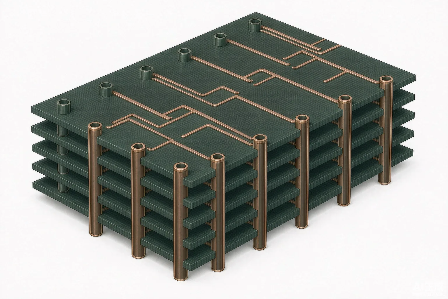
An HDI board is defined by laser-drilled microvias: holes around 0.1 mm that a mechanical drill cannot produce reliably. The stage number counts how many times those microvias are formed and laminated. A 1-stage build drills the outer layer to the adjacent inner layer once. A 2-stage build laminates a first pair of microvias into the panel, then drills and laminates a second pair on top. A 3-stage build repeats the cycle a third time.
In other words, the stage number is the number of laser passes, and every pass drags a lamination cycle behind it. That single fact explains almost everything else about HDI: why cost rises faster than layer count, why registration tolerance gets harder to hold, and why yield risk climbs with each additional stage.
The ceiling of this counting system is any-layer HDI, where a microvia is formed between every pair of adjacent layers and stage counting stops making sense. The practical boundary between “3-stage” and “any-layer” is exactly there: once every layer pair has its own laser via, the concept of stacking passes no longer applies.
HDI Stages Explained: 1-Stage, 2-Stage and 3-Stage Build-Ups
1-Stage HDI
A single laser pass from the outer layer to layer 2, on one or both sides. Common configurations are 4-layer 1-stage, 6-layer 1-stage and 8-layer 1-stage. There is no stacked via structure, so no via filling is normally required, and registration is the easiest of the three to hold. Most fine-pitch fan-out problems are solved here and do not need to go further.
2-Stage HDI
Two laser passes and three lamination cycles. The second pass allows the microvia to reach deeper into the board, so fewer routing layers are needed for the same escape density. At this point the via relationship starts to matter: microvias can be staggered (offset, separated by a copper landing pad) or stacked (aligned directly on top of one another). Stacked microvias require resin plugging plus copper-filled plating to keep the stack electrically and mechanically sound, which adds process steps and a reliability validation set.
3-Stage HDI and Any-Layer
Three laser passes and four or more lamination cycles. This is where dense die stacking and package-substrate-style routing live. Beyond 3-stage, the industry stops counting stages and switches to any-layer terminology, because the structure is uniform rather than stacked. Typical applications move from phone sub-boards and camera modules at 1-stage, through SSDs, core boards and AI edge terminals at 2-stage, to die stacking, package substrates and high-speed modules at 3-stage and above.
One useful sanity check before going further: stage count and layer count are independent variables. An 8-layer 2-stage and a 10-layer 1-stage can solve the same routing problem, and the cheaper answer is not always the one with fewer layers.
Process Parameters Compared Across HDI Stages
The table below is the practical difference between HDI stages at the process level. Values are production capability; limits marked “by review” are quoted per order after engineering assessment.
| Parameter | 1-Stage HDI | 2-Stage HDI | 3-Stage HDI |
|---|---|---|---|
| Lamination cycles | 2 (including the inner-layer sub-board) | 3 | 4 or more |
| Laser drilling passes | 1 | 2 | 3 |
| Microvia diameter | 0.1 mm | 0.1 mm | 0.1 mm (0.076 mm by review) |
| Minimum line / space | 2/2 mil (1.8/1.8 mil on prototypes) | 2/2 mil (1.8/1.8 mil on prototypes) | 2/2 mil (1.8/1.8 mil on prototypes) |
| Via relationship | Not applicable | Staggered, or stacked with resin plugging and copper filling | Mainly stacked; plugging and filling are standard |
| Blind via aspect ratio | 1:1 | 1:1 | 1:1 (1:1.2 by review) |
| Typical applications | Phone sub-boards, camera modules, consumer devices | SSD modules, core boards, AI edge terminals | Die stacking, package substrates, high-speed modules |
Two rows carry most of the risk. The first is the via relationship: from 2-stage onward, stacked microvias demand resin plugging followed by copper-filled plating, which is where void-free filling decides yield. The second is interlayer registration: each lamination cycle adds accumulated tolerance, and holding it is the real reason high-stage HDI is difficult to manufacture, not the laser drilling itself.
How HDI Stages Change Cost
Cost does not scale linearly with stage count. Each additional stage multiplies three separate cost factors: laser drilling machine time, lamination cycles, and yield loss absorbed into unit price. A scrapped 3-stage panel has already consumed far more value than a scrapped through-hole panel, so the loss per defect is larger even when the defect rate is comparable.
| Build | Relative cost versus an 8-layer through-hole baseline | Dominant cost driver |
|---|---|---|
| 8-layer through-hole baseline | Baseline | Layers and panel utilisation |
| 8-layer 1-stage HDI | Roughly +30% to +60% | One laser pass and one extra lamination cycle |
| 8-layer 2-stage HDI | Roughly +60% to +100% | Second laser pass, stacked-via plugging and filling |
| 12–14 layer 3-stage HDI | Roughly +100% and upward, quoted per order | Third laser pass, four or more lamination cycles, registration yield |
Read the multipliers as a rule of thumb rather than a price list. Actual quotations depend on panel size, quantity, copper weight, finish and the specific via structure, and they are confirmed at engineering review against the actual Gerber data.
The commercial consequence is straightforward: de-escalating a stage is almost always worth attempting before committing. Replacing a stacked 2-stage design with a staggered 2-stage design removes the plugging and filling operations. Splitting the routing so that part of the escape density is handled by one additional through-hole layer can turn a 2-stage requirement into a 1-stage build. Both routes usually beat paying for a stage that the design does not strictly need.
Prototype Lead Time by HDI Stage
Lead time follows lamination cycles almost mechanically. Each additional stage adds laser drilling and a press cycle that cannot be compressed by scheduling alone, because the panel must physically go through the line again. Typical prototype lead times for HDI stages look like this.
| Build | Typical prototype lead time | Note |
|---|---|---|
| 8-layer through-hole | Around 9 working days | No laser drilling |
| 4-layer 1-stage HDI | Around 10 working days | Inner-layer sub-board plus one laser pass |
| 6-layer 1-stage HDI | Around 12 working days | One laser pass, more inner routing |
| 8–10 layer 2-stage HDI | 17–18 working days | Two laser passes, stacked-via option |
| 12–14 layer 3-stage HDI | 22–24 working days | Three laser passes, four or more lamination cycles |
As a planning rule, each additional HDI stage typically adds 3–5 working days to a prototype build. Expedited schedules are reviewed per order against current capacity and material availability, and the confirmed date is issued with the quotation. Full detail on standard and compressed windows is published on our PCB lead time page.
This is why HDI stage decisions belong in the schematic and layout phase, not in procurement. Moving from 1-stage to 2-stage late in the project can add two working weeks and a significant cost multiple to a schedule that no amount of expediting can recover.
Choosing Between HDI Stages by BGA Pitch and Layer Count
Two inputs decide the stage: the finest pitch you have to escape, and whether you can afford another layer. Minimum BGA pad diameters are 0.2 mm as a general rule, with 0.15 mm available on mid-volume orders.
| Design situation | Recommended stage | Reasoning |
|---|---|---|
| BGA pitch above 0.65 mm, escape density solvable by adding layers | Through-hole board; no HDI needed | Adding a layer pair costs less than adding a laser pass |
| BGA pitch 0.5–0.65 mm, dense pad escape or via-in-pad required | 1-stage microvia | A single laser fan-out resolves the escape |
| BGA pitch around 0.4 mm, or layer count must come down | 2-stage microvia | Two microvia passes buy routing density and remove layers |
| BGA pitch 0.35 mm and below, die stacking, package-substrate geometry | 3-stage or any-layer | Only multiple microvia passes can escape the array |
Via-in-pad is the second lever worth knowing about. It places the via directly in the component pad, which removes the short stub that otherwise costs routing space. It is available with either resin plugging or copper-filled plating, and the choice between those two follows the assembly requirement rather than preference. Reference builds using these structures include our 10-layer 2-stage HDI prototype, the 14-layer 2-stage HDI prototype and the 12-layer 1-stage HDI board.
Stacked vs Staggered Microvias: Where Reliability Is Decided
Once a design reaches 2-stage, the via relationship becomes the single most consequential process decision. In a staggered arrangement, each microvia lands on a copper pad offset from the via below it. The copper between the vias distributes mechanical stress, so no additional filling is required. In a stacked arrangement, the microvias sit directly on top of each other and the stack must be resin plugged and copper filled to avoid trapped voids and plating voids.
Stacked microvias save routing area because they occupy one vertical column rather than a diagonal footprint. That is often exactly what a dense escape needs. The trade-off is a longer process chain: plugging, curing, planarisation and filling all sit between drilling and the next lamination cycle, and each one is an opportunity for a void that later shows up in reliability testing.
If the layout allows a diagonal offset, a staggered structure is usually the more economical and easier-to-validate answer. If it does not, stacked microvias are workable, but they should be specified deliberately and inspected for fill quality rather than assumed.
Common Mistakes When Specifying HDI Stages
- Assuming every small board needs HDI. Board area is not the constraint; escape density is. If a smaller outline with an extra layer pair meets the requirement, that is normally cheaper than a second laser pass.
- Treating stage count as a quality grade. A 1-stage board built to IPC Class 3 is a higher-reliability product than a careless 3-stage board. Stage count describes geometry, not reliability.
- Confusing stage count with layer count. They are independent. 8-layer 2-stage and 10-layer 1-stage are two answers to the same problem, and they should be quoted side by side before choosing.
- Leaving impedance requirements until after the stackup is frozen. Controlled impedance on an HDI build depends on the dielectric thickness between the reference plane and the signal layer, so the stackup and the impedance target have to be agreed together. Our process capability page lists the tolerances we hold.
- Specifying a stage before the fab has reviewed the Gerber data. A stackup review usually identifies where a stage can be removed. It costs nothing at quotation stage and a great deal after tooling has started.
Manufacturing Capability Behind These HDI Stages
1-stage through any-layer HDI is standard production here, with 4+N+4 stackups supported as a routine configuration. Laser-drilled microvias start at 0.1 mm, with 0.076 mm available by engineering review. Minimum line and space is 2/2 mil in production and 1.8/1.8 mil on prototype and sample orders, and blind via aspect ratio is held at 1:1, with 1:1.2 quoted per order.
Via-in-pad is supported with resin plugging and with copper-filled plating, and both routes are validated by cross-section and electrical test rather than by visual inspection alone. Boards are built to IPC Class 2 or Class 3 as specified, under ISO 9001:2015 quality management and IATF 16949 for automotive programmes, with UL recognition and RoHS and REACH compliance as standard.
Because stage selection is a stackup decision rather than a catalogue choice, the fastest way to a firm answer is to send the Gerber data with the target BGA pitch, layer count and quantity. The engineering team returns a per-stage assessment showing which stage is manufacturable at what cost multiple and what lead time, so the decision is made on data rather than on a default. That review is part of our PCB manufacturing service, from prototype through to production volume, and it is the point at which most unnecessary stages get removed.
Frequently Asked Questions About HDI Stages
What is the difference between 1-stage and 2-stage HDI?
A stage is one laser-drilling and lamination cycle for microvias. 1-stage HDI forms a single microvia from the outer layer to the adjacent inner layer, using two lamination cycles. 2-stage HDI forms microvias, laminates, then forms a second set, using three lamination cycles. The second stage allows microvias to reach deeper into the board, which increases routing density and can reduce the number of layers required. For the full parameter envelope behind these build-ups, see our HDI PCB technology guide.
How do I choose between HDI stages?
Start from BGA pitch. Above 0.65 mm, a through-hole board is usually sufficient. Between 0.5 mm and 0.65 mm, 1-stage microvias are typically enough. Around 0.4 mm, or when layer count must be reduced, 2-stage is the usual answer. At 0.35 mm and below, or with die stacking, 3-stage or any-layer construction is required. Always compare a de-escalated option before committing.
Which HDI stages does the factory build?
1-stage through any-layer HDI are standard production, with 4+N+4 stackups supported. Laser microvias start at 0.1 mm with 0.076 mm available by engineering review, minimum line and space is 2/2 mil in production and 1.8/1.8 mil on prototypes, and via-in-pad is available with resin plugging or copper-filled plating. The design rules that follow from these limits are covered in our HDI stackup and design rules.
How much does each additional HDI stage cost?
Each additional stage typically raises cost by roughly 30% to 100% compared with the stage below it, driven by laser drilling machine time, an extra lamination cycle, via plugging and filling where stacked microvias are used, and yield loss absorbed into unit price. The exact multiple depends on panel size, quantity, copper weight and via structure, and is confirmed against the Gerber data at quotation.
How long does a 2-stage or 3-stage HDI prototype take?
An 8 to 10 layer 2-stage HDI prototype typically runs 17 to 18 working days, and a 12 to 14 layer 3-stage prototype typically runs 22 to 24 working days. As a planning rule each additional stage adds about 3 to 5 working days. Compressed schedules are reviewed per order against capacity and material availability.
Why does a 3-stage HDI board cost so much more than 1-stage?
Four factors compound. Lamination cycles double or more, laser drilling machine time accumulates with each pass, stacked microvias require resin plugging and copper-filled plating, and interlayer registration becomes harder to hold across more cycles, so yield loss carries a higher value per scrapped panel. High-stage boards also cost far more to scrap because more processing has already been invested.
What is the minimum trace width on an HDI board?
2/2 mil is the standard production minimum, and 1.8/1.8 mil is available on prototype and sample orders subject to engineering review. Laser microvia diameter starts at 0.1 mm, with 0.076 mm quoted per order, and blind via aspect ratio is held at 1:1, with 1:1.2 available by review.
Should a stacked or staggered microvia structure be used?
Use staggered microvias wherever the layout allows, because the offset landing pad distributes mechanical stress and no via filling is required. Use stacked microvias when routing density leaves no alternative; they save area, but they must be resin plugged and copper filled, which adds process steps and makes void-free fill the critical quality control point. The geometry rules that govern both structures are defined in IPC-2226, the HDI microvia design standard maintained by the Global Electronics Association.
Get Your HDI Stackup Reviewed Before You Commit to a Stage
Send the Gerber data together with the target BGA pitch, layer count and quantity. The engineering team returns a stage-by-stage assessment showing which HDI build is manufacturable, what each option does to cost and what prototype lead time it carries, so the choice is made on data instead of on a default.
From 4-layer 1-stage and 6-layer 2-stage builds through to 10-layer industrial control HDI, samples and production volumes run from the same data set.