Book Appointment Now

How any-layer HDI stacks and interconnects every layer pair, how the drill-fill-cap loop runs, and when it beats 2-stage HDI on density.
Any-Layer HDI Explained: ELIC Stackup, Process Flow and When to Use It
When a smartphone mainboard has to swallow an application processor, memory stacks, RF front ends and power management in a few square centimetres, sequential HDI eventually runs out of escape routing. Any-layer HDI — often called ELIC, for every-layer interconnect — removes the last structural restriction: a laser microvia can connect any adjacent copper pair, not just the first one or two build-up stages.
This article explains how the stackup is organised, how the drill-fill-cap manufacturing loop works pair by pair, where any-layer HDI sits against 1-, 2- and 3-stage constructions on density and cost, and the DFM rules that decide whether your design is buildable. It is written for hardware engineers and sourcing teams evaluating whether the density gain justifies the process premium.
Table of Contents
- What Any-Layer HDI Means (and Where the ELIC Name Comes From)
- How an Any-Layer HDI Stackup Is Organized
- The Laser-Drill, Fill and Cap Loop That Builds Every Pair
- Any-Layer HDI vs Sequential 1-, 2- and 3-Stage Builds
- Design Rules and DFM Limits That Decide Feasibility
- When the Density Gain Justifies the Cost
- Applications That Depend on Any-Layer Interconnect
- Cost and Lead-Time Expectations, Stated Honestly
- How to Qualify a Factory for Any-Layer Builds
- FAQ
- Have Your Any-Layer HDI Stackup Reviewed Before Release
What Any-Layer HDI Means (and Where the ELIC Name Comes From)
In a conventional sequential build, microvias exist only in fixed positions: stage one connects L1–L2, stage two connects L1–L3 through a stacked pair, and so on. Any-layer HDI removes that staircase. Every adjacent copper pair in the board is treated as a potential interconnect site, drilled by laser and filled with copper, so a signal can move between any two layers through short, stacked vertical jumps.
The name ELIC — every-layer interconnect — describes the same construction from the process side: instead of building stages around a rigid sub-composite, the board grows one copper pair at a time, each pair receiving its own laser drilling, plating fill and capping before the next lamination. The result is the densest vertical routing fabric available in volume PCB production, and the reason it appears in flagship phones, camera modules and dense processor modules.
The practical consequence for a designer: escape a 0.35 mm-pitch BGA in four rows instead of two, put decoupling vias directly in pads on every layer, and shorten critical vertical transitions dramatically. The consequence for the schedule and the budget: every layer pair adds a full process loop, which is why this construction earns its premium only where density truly binds.
How an Any-Layer HDI Stackup Is Organized
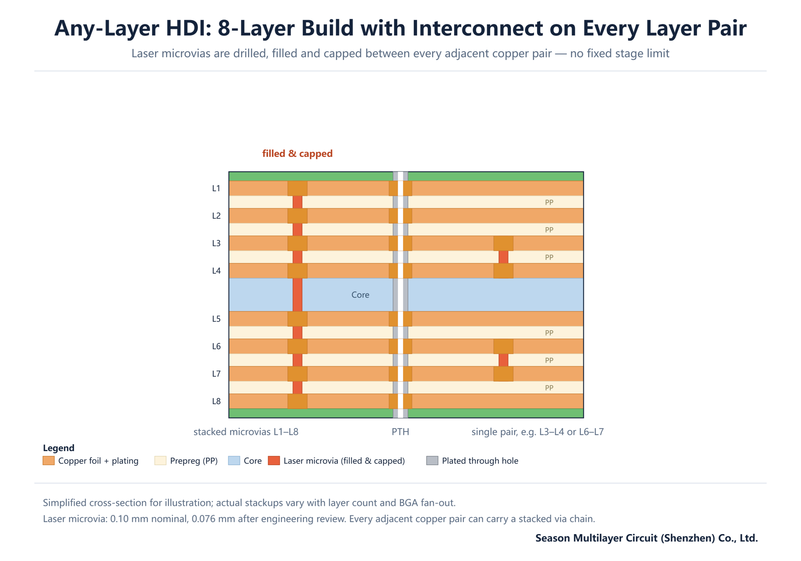
An 8-layer any-layer HDI build is the classic teaching example. The copper pairs are laminated one on top of another, with prepreg between each pair and a core (or a thicker laminated centre) providing mechanical stability in the middle of the construction:
| Layer | Function | Dielectric between it and the next layer |
|---|---|---|
| L1 | Outer signal (component side) | Prepreg (PP) |
| L2 | Inner signal | Prepreg (PP) |
| L3 | Inner signal | Prepreg (PP) |
| L4 | Inner signal | Core (centre laminated backbone) |
| L5 | Inner signal | Prepreg (PP) |
| L6 | Inner signal | Prepreg (PP) |
| L7 | Inner signal | Prepreg (PP) |
| L8 | Outer signal (solder side) | Solder mask |
Because every adjacent pair carries a laser-drilled, filled and capped microvia, the stackup above supports a continuous via chain from L1 to L8 plus any single-pair hop — L3–L4, L6–L7, whichever the routing needs. Layer counts above eight follow the same rhythm; the construction just repeats the loop more times, and the lamination cycle count grows with it.
The Laser-Drill, Fill and Cap Loop That Builds Every Pair
Each layer pair goes through the same core loop. First, laser drilling opens the microvia — 0.10 mm nominal, down to 0.076 mm after engineering review. The hole is cleaned, then electroplated with copper until it fills solid; a fully filled microvia is what makes stacking on top of it reliable, because an empty or voided via collapses under the next lamination. The filled via is then capped with the plating of the next copper layer, and the whole sub-assembly is laminated again.
That loop is why copper-filled via plating quality decides the yield of the entire construction: a single void at layer three surfaces as a field failure after six more lamination cycles. Registration accuracy matters just as much, since each new pair must land its microvias on the buried pads below — our layer-to-layer registration guide explains how factories hold that window.
In designs that place microvias directly under BGA or capacitor pads, the filled-and-capped structure doubles as the pad itself — the standard via-in-pad practice. On an any-layer build this is not an exotic option but the default routing economy: vias in pads on every layer pair are what release the escape channels around fine-pitch parts.
Any-Layer HDI vs Sequential 1-, 2- and 3-Stage Builds
The honest comparison is structural, not emotional. Sequential stages and any-layer differ in how many vertical hops exist, how many lamination cycles that implies, and what it costs:
| Aspect | 1-Stage | 2-Stage | 3-Stage | Any-layer (ELIC) |
|---|---|---|---|---|
| Microvia span per side | L1–L2 | L1–L3 | L1–L4 | Every adjacent pair |
| Stacked via levels | 1 | 2 | 3 | Up to one per layer pair |
| Lamination cycles | 2 | 3 | 4+ | One per layer-pair loop |
| Escape under fine-pitch BGA | 2 rows | 3–4 rows | 4+ rows | Full grid, all layers |
| Relative cost | Base | +30–100% | Higher again | Highest — typically above a 3-stage build |
| Typical territory | 4–8 layers | 8–12 layers | 10–16 layers | 8–16 layers, density-bound designs |
Read the table as a decision ladder, with the 1-, 2- and 3-stage HDI structures as the rungs below. Most dense consumer boards stop at 2-stage because the escape problem is solved there; any-layer is for the case where even a full 3-stage build cannot release the routing — usually the highest layer counts in the smallest board area, with fine-pitch parts on both sides.
Design Rules and DFM Limits That Decide Feasibility
Any-layer HDI lives inside a tight process window, and the DFM conversation is most productive when the design arrives inside it. The working rules we apply daily: laser microvias at 0.10 mm nominal (0.076 mm on review), a via aspect ratio around 1:1, minimum line width and spacing of 2/2 mil (1.8/1.8 mil on prototype orders), and stacked microvias kept filled, capped and staggered-or-stacked according to the pad geometry. For HDI-specific layout guidance, IPC’s standards library includes the design guides most engineering teams reference.
Two rules deserve extra weight. First, keep the copper balance symmetric through the build — every added pair shifts the laminate schedule, and an unbalanced construction warps. Second, respect the microvia pad-to-trace geometry: because each pair is laminated separately, a design that violates the pad targets does not just fail inspection at the end, it fails at layer three and takes the whole panel with it.
None of these rules is secret, and none is negotiable in the direction of risk. The boards that ship on schedule are the ones whose designers treated the stackup review as a design input, not a final approval step. If you are weighing stacked against staggered microvia structures for a less aggressive build, our stacked vs staggered vias comparison covers the trade-offs pair by pair.
When the Density Gain Justifies the Cost
Any-layer HDI earns its premium in three situations. One: fine-pitch components whose escape routing physically cannot close on a 2-stage build, no matter how cleverly the channels are arranged. Two: extreme layer-to-area ratios, where adding two more sequential stages would cost nearly as much as any-layer while delivering less routing freedom. Three: vertical transitions that must stay short for signal-integrity reasons — a filled via chain hops between adjacent layers instead of reaching a buried layer and back.
- Escape-closure test: can your worst BGA fan out within a 2-stage construction? If yes, stop there
- Layer-count test: would a 3-stage build at two extra layers cost about the same but route worse? Any-layer wins those
- Signal-integrity test: do critical nets need the shortest possible vertical path? Filled any-layer chains beat deep via stubs
- Volume test: any-layer’s per-board premium amortises better at scale; for small batches, reconsider whether the density is truly required
The failure mode to avoid is choosing any-layer for prestige. The construction is a routing tool with a price tag; when the escape math closes on a cheaper ladder rung, the honest recommendation is the cheaper rung.
Applications That Depend on Any-Layer Interconnect
Flagship smartphones are the reference application: application processors with 0.3–0.35 mm pitch, stacked memory and RF modules on a mainboard that shrinks every generation. Wearable and hearable products compress the same problem into less area — compact audio boards such as our 6-layer 2-stage HDI headphone PCB solve their routing with a sequential build, while the denser true-wireless and AR-class devices move to every-layer interconnect as the part count grows.
Camera modules and compact sensor packages form the second cluster: image pipelines want short, clean vertical transitions under the sensor connector, and any-layer constructions deliver them. Computing and network modules — dense processor cores, switch chips, high-pin-count SoMs — are the third cluster, where the same physics that drives 12-layer 1-stage HDI core boards eventually drives the densest members to every-layer interconnect. Portable diagnostic and industrial instruments round out the list wherever board area carries a system-level cost.
Across all of them the pattern repeats: the construction follows the pin density, not the industry. If your next design halves the board area of its predecessor while keeping the silicon, it is probably heading down this ladder.
Cost and Lead-Time Expectations, Stated Honestly
Priced against the same layer count, any-layer HDI lands above a 3-stage sequential build, which itself carries a 30–100% premium per stage over a 2-stage construction. The exact multiple depends on layer count, microvia count per layer, laminate class and fill requirements — which is why the only meaningful comparison is a quotation built on your actual stackup, not a category-to-category guess.
Lead time follows the same logic: every layer pair adds a lamination cycle, drilling pass and plating loop, so an any-layer prototype takes longer than a 2-stage build of the same layer count. Treat any timeline given before engineering review as an estimate; the confirmed schedule comes out of the reviewed stackup, with the microvia count and fill requirements known. What we commit to is the review itself — fast, in writing, with the constraints stated.
How to Qualify a Factory for Any-Layer Builds
Because yield is decided inside the drill-fill-cap loop, qualification should probe the loop, not the brochure. Ask for: laser drilling equipment specs and the smallest microvia drilled in routine production; fill-plating capability and cross-section evidence of filled microvias; registration capability between stacked vias; and the lamination schedule for a build like yours. A factory running any-layer in volume answers these without hesitation.
Data quality is the other half of qualification. Send complete, attributed Gerber data with the stackup request, and check that the response comes back as a dielectric-by-dielectric table with per-layer impedance targets and process notes — the same discipline we apply to 10-layer 2-stage HDI prototypes and every denser build above them. For the wider capability picture, our HDI capability guide lists what to read between the lines of any capability sheet.

Group scale matters at this construction level: capacity reserved for HDI loops, engineering review depth and process audit cadence all correlate with the maturity of the production floor. The HDI PCB technology overview on our corporate site summarises the group’s HDI position if you need the background for an internal sourcing memo.
Frequently Asked Questions
What is any-layer HDI?
Any-layer HDI is a high-density interconnect construction in which a laser-drilled, copper-filled microvia can be placed between any adjacent copper pair — not only within the first build-up stage. The board grows one layer pair at a time, each pair receiving its own drill, fill, cap and lamination loop.
Is ELIC the same thing as any-layer HDI?
Yes. ELIC stands for every-layer interconnect and describes the identical construction from the process side: every adjacent layer pair is interconnected by stacked, filled and capped laser microvias. The two terms are used interchangeably in datasheets and quotations.
How many lamination cycles does an any-layer build require?
One full lamination loop per layer pair. An 8-layer any-layer board therefore runs more lamination cycles than a 3-stage build of the same layer count, which is the structural reason behind both its routing freedom and its cost and lead-time premium.
What design rules apply to any-layer microvias?
Laser microvias at 0.10 mm nominal (0.076 mm after engineering review), an aspect ratio around 1:1, fully filled and capped vias when stacked, and minimum line width and spacing of 2/2 mil in routine production. Via-in-pad with copper fill is standard practice to release escape routing under fine-pitch parts.
When is any-layer HDI worth it instead of 2-stage HDI?
When the escape routing of your densest components cannot close on a 2-stage build, when the layer-to-area ratio demands more vertical hops than sequential stages provide, or when critical nets need the shortest possible vertical transitions. If a 2-stage construction closes the fan-out, it remains the economical choice.
How much more does any-layer HDI cost than a sequential build?
It lands above a 3-stage sequential build of the same layer count, which itself carries a 30–100% premium per added stage over 2-stage. The exact multiple depends on layer count, microvia density and fill requirements, so the reliable comparison is a quotation on your actual stackup.
What data does the factory need to quote an any-layer build?
Complete Gerber and drill files, the layer count and total thickness window, the microvia plan (which pairs carry vias, stacked or single), BGA pitch and pin counts for the densest parts, and the laminate preference. With those inputs, engineering review returns a buildable stackup with per-layer process notes.
Have Your Any-Layer HDI Stackup Reviewed Before Release
Send your Gerber data, layer count and the microvia plan, and our engineering team will return a pair-by-pair feasibility review — lamination schedule, fill and registration checks, and the honest answer on whether a cheaper sequential stage closes your routing. Start through our PCB manufacturing services page, or read more HDI guides in the PCB basics library.