Book Appointment Now

Seven common PCB defects — opens and shorts, thin via walls, mask blisters, pad lift and warpage — with root causes, acceptance limits and prevention.
PCB Defects: 7 Common Failure Modes, Causes and Process Fixes
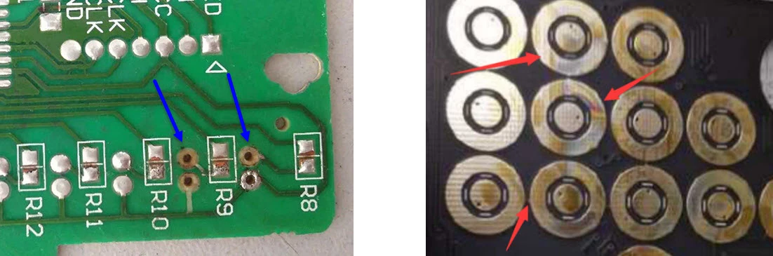
Most scrap and rework on a multilayer board traces back to a short list of recurring PCB defects: open or shorted traces, thin or voided via walls, solder mask blisters, lifted or oxidized pads, and warped panels. For a buyer, the hard part is not knowing the names — it is knowing which process step owns each failure, what an acceptable limit looks like, and what evidence to demand when a batch goes wrong. This guide walks through the seven failure modes that account for most field returns, with root causes, acceptance criteria and prevention measures for each.
Every acceptance judgement below follows the framework of IPC-A-600 and IPC-6012, the workmanship standards used on production lines worldwide. That matters commercially: a defect is not a feeling, it is a measurable nonconformance against an agreed class — and the class is set in your purchase order, not discovered after the fact.
Table of Contents
- How PCB Defects Are Classified: Reject, Rework or Use-As-Is
- How PCB Defects Are Caught Before Shipment
- Open and Short Circuits at Trace Level
- Thin or Voided Via Walls After Drilling and Plating
- Solder Mask Blisters, Peeling and Skipped Areas
- Pad Lift, Pad Oxidation and Solderability Loss
- Bow, Twist and Warpage Acceptance Limits
- Annular Ring Breakout and Layer Registration
- Delamination, Measling and Base-Material Defects
- Mapping PCB Defects to the Process Step That Owns Them
- When the Root Cause Is in the Design Files, Not the Line
- A Practical Incoming Inspection Checklist
- Prevention, Acceptance Limits and What to Specify
- FAQ
- Get a DFM and Process Review Before You Order
How PCB Defects Are Classified: Reject, Rework or Use-As-Is
A PCB defect is any characteristic of a finished board that fails the acceptance criteria of the agreed inspection class — typically IPC Class 2 for industrial and consumer products, Class 3 where downtime or repair cost is unacceptable. The same physical feature can be a scrap condition, a reworkable condition, or a use-as-is condition depending on the class and on where it appears. A small solder mask blemish that does not reduce conductor spacing may be acceptable on a Class 2 board and marginal on a Class 3 board; a plated through-hole with copper below the minimum average thickness is a reject in both.
Classification is what turns quality arguments into engineering conversations. When a supplier and a customer agree in advance which standard and which class govern acceptance, a disputed board can be evaluated against published criteria instead of negotiated by email. The overview below maps the seven failure modes covered in this article.
| Failure mode | What it looks like | Primary root cause |
|---|---|---|
| Open or short circuit | Trace discontinuity, or unintended connection between nets | Etch control, drilling burrs, plating nodules, contamination |
| Thin or voided via wall | Copper plating in the barrel below minimum, or a void seen in cross-section | Drill smear not fully removed, plating chemistry out of window |
| Solder mask blister or peel | Raised bubbles, or mask lifting and exposing bare copper | Contamination, under-cure, moisture outgassing |
| Pad lift or pad oxidation | Pad separating from laminate, or discolored, non-wettable pads | Overheating, contaminated storage, surface finish faults |
| Bow and twist (warpage) | Panel not flat; corners lift off the reference surface | Unbalanced copper distribution, wrong lamination and cure profile |
| Annular ring breakout | Hole not centered in its pad; tangency or breakout on one side | Layer-to-layer registration drift, drill entry/exit error |
| Delamination and measling | Separation between layers or blisters inside the laminate | Moisture, lamination pressure or temperature out of window |
How PCB Defects Are Caught Before Shipment
None of these failure modes should reach you undiscovered. A capable line uses a chain of overlapping inspection points, each tuned to the defect class it can see best. Electrical test catches opens and shorts that no camera can see; automated optical inspection after etch catches trace-level geometry faults; X-ray sees the hidden joints and hidden geometry that surface cameras cannot; and micro-sectioning — cutting a coupon from a panel and polishing it — is the only method that proves what the inside of a via wall actually looks like.
The important distinction for a buyer is coverage versus sampling. Electrical test is cheap enough to run 100% on production panels, which is why a shorted inner layer or an open trace should never ship. Micro-sectioning is destructive, so it runs on coupons from each manufacturing lot — which is why the coupon program and the lot traceability behind it are worth checking on an audit rather than assuming.
- Inner-layer AOI after etch — trace width, spacing and open/short on every inner layer before lamination
- Post-lamination drilling checks — hole position, drill smear control, hole count verification
- Electrical test (flying probe for prototypes, test fixtures for volume) — 100% open/short verification
- Automated optical inspection on outer layers — mask registration, exposed copper, surface blemishes
- Micro-section coupons — plating thickness in the barrel, layer alignment, laminate integrity
- Final visual per IPC-A-600 — workmanship items that machines judge inconsistently
Open and Short Circuits at Trace Level
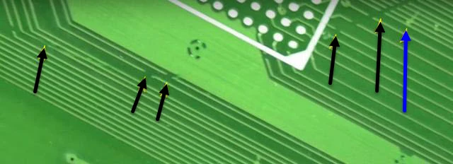
Opens and shorts are the most classic pair of PCB defects, and both are process problems before they are material problems. An open appears when etching removes too much copper — aggressive etch chemistry, long dwell time, or a trace designed at the limit of the process window. A short appears when copper that should have been etched away survives: a bridging sliver between traces, a drilling burr that connects adjacent layers, or a nodule of plating copper growing where the resist was damaged.
Design margin decides how much of this the line can absorb. Traces and gaps sized at the minimum the fabricator quotes leave zero room for normal process drift; adding even a little spacing moves the design back into the robust middle of the window. On the production side, inner-layer AOI before lamination is the control point that catches both conditions at the cheapest moment — an open caught before lamination costs one layer; caught at final test, it costs a finished panel.
Thin or Voided Via Walls After Drilling and Plating
A plated through-hole or via is only as good as the copper on its barrel wall. Two related defects dominate: copper below the minimum average thickness, and voids — spots where the plating never formed at all. The causes cluster around the desmear and plating steps: drill smear left on the wall prevents adhesion, current density set too high builds copper unevenly at the mouths of the hole, and bath chemistry outside its control window produces thin deposits in the middle of high aspect-ratio holes.
The reason this defect matters more than its size suggests is latency. A via with marginal barrel copper can pass electrical test on the day it is made and then crack open after hundreds of thermal cycles in the customer’s product — which is exactly the failure mode that reliability qualification testing is designed to expose before shipment. There is no practical field repair for a voided barrel; the only fixes are coupon-based detection, scrap, and a process correction. That is why serious buyers treat micro-section reports as lot-level evidence, not paperwork.

Solder Mask Blisters, Peeling and Skipped Areas
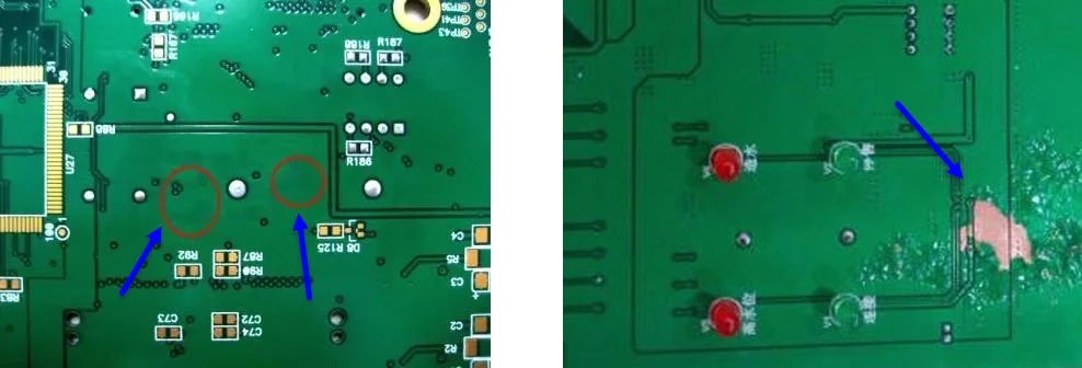
Solder mask is the board’s protection layer, and its two characteristic PCB defects sit at opposite ends of the severity scale. Blisters — small raised bubbles — usually come from moisture or solvent outgassing during cure, or from contamination on the copper before coating. Peeling and skipped areas are worse: when the mask lifts and exposes copper, the bare conductor oxidizes, solderability degrades, and in humid environments corrosion proceeds under the remaining mask edge.
Acceptance is contextual, which is what makes this defect the most argued-over item on final visual inspection. Under Class 2 criteria, a localized blister that does not reduce conductor spacing below the minimum and does not compromise solderable areas can be acceptable; peeling that exposes copper is not. Prevention is unglamorous and effective: clean copper before coating, bake out moisture before and during cure, and hold the mask thickness in a controlled range — including on the walls of any hole that is plugged rather than tented, as covered in the via plugging methods comparison.
Pad Lift, Pad Oxidation and Solderability Loss
Pads fail in two distinct ways. A lifted pad is a mechanical failure: the pad separates from the laminate, usually because of excessive local heating during assembly rework, or because the laminate itself was weakened by a lamination fault. Pad oxidation is a chemical failure: the finish or the bare copper has reacted with the environment, and solder no longer wets the surface reliably. The two look similar at arm’s length and have completely different root causes, which is why a root-cause letter that just says “bad pads” settles nothing.
Oxidation is usually a storage and surface-finish story rather than a fabrication one. Every finish has a shelf life — ENIG solderability and its black-pad failure mode being the most documented example — and humidity-accelerated ageing will outdate a board long before its calendar expiry. Vacuum-packed storage with desiccant, reasonable warehouse humidity, and first-in-first-out rotation prevent most of it. Lifted pads, on the other hand, are prevented at design time: generous pad-to-laminate adhesion area, and a rework temperature policy that respects the laminate’s limits.
Bow, Twist and Warpage Acceptance Limits
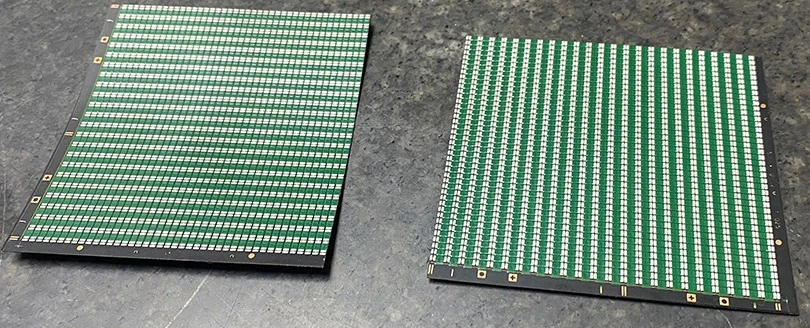
Warpage is the defect class that surfaces at assembly, not at final visual inspection — which is precisely why it is so expensive when it slips through. A warped panel will not sit flat in the printer or the pick-and-place carrier, and during reflow the board flexes while the solder solidifies. The standard acceptance limit under IPC-6012 is 0.75% of the diagonal for boards carrying surface-mount devices and 1.5% for boards without them; for dense SMT panels the practical target is tighter still.
The dominant causes are asymmetry, not bad luck: copper distributed unevenly layer to layer, a stackup with dissimilar symmetry above and below the neutral axis, or a press and cure cycle that locks in residual stress. All three are design-and-process problems that can be engineered out before the panel is ever pressed — the balanced stackup and copper-balance design rules cover the mechanics in detail. The photo below shows the kind of visible bow that fails the limit at a glance.
Annular Ring Breakout and Layer Registration
Every via is supposed to land inside its pad with copper surrounding it on all sides — the annular ring. When layer-to-layer registration drifts or the drill wanders, the hole ends up tangent to the pad edge or breaking out of it. A breakout on a non-functional side may be acceptable by criteria; a breakout that severs the connection between the barrel and the trace is a hard defect, and marginal rings pass test today and fail in the field.
The design lever is simple: specify an annular ring large enough to absorb realistic registration tolerance for the layer count in question, especially on Class 3 work where the required minimum ring is stricter. The production lever is registration control — material movement compensation per layer, tooling accuracy, and verification through the same micro-section coupons that measure plating. Registration is also one of the process capabilities that separates a commodity line from a high-reliability multilayer production line, where 8-layer and above builds live or die by layer alignment.
Delamination, Measling and Base-Material Defects
Delamination is separation between layers or between copper and laminate; measling is the fine internal blistering that shows as white spots in the laminate. Both are laminate-integrity defects, and both trace back to a short list of causes: moisture absorbed into the base material before or during lamination, press pressure or temperature outside the material’s window, and chemically aggressive processing after lamination.
Material selection and incoming material quality carry more of this risk than most buyers expect — resin system, glass style and storage age all change how forgiving a laminate is. The laminate quality and incoming inspection guide covers what to check before material enters production, and the PCB materials and laminates pillar guide explains how resin systems differ in the behaviours that drive these defects.
Mapping PCB Defects to the Process Step That Owns Them
When a batch fails, the useful question is never “what is the defect” but “which process step owns it”. The mapping below is the one production engineers use to route a nonconformance to the station that can actually prevent it. It is also the right skeleton for a root-cause or corrective-action report: defect, evidence, owning step, control that failed, and the change that prevents recurrence.
| Process step | Defects it owns | Primary control point |
|---|---|---|
| Imaging and etch | Opens, shorts, trace width violations | Inner-layer AOI, etch chemistry monitoring |
| Drilling | Smear, burrs, misregistration leading to breakout | Drill parameter control, entry/exit material, tool wear limits |
| Desmear and plating | Thin or voided via walls, poor adhesion | Bath analysis, current density, coupon micro-sections |
| Lamination | Delamination, measling, bow and twist | Moisture control, press cycle, material pre-treatment |
| Solder mask | Blisters, peeling, skipped areas, mask on pads | Surface cleanliness, cure profile, thickness control |
| Surface finish | Oxidation, solderability loss, finish contamination | Bath control, storage, shelf-life management |
| Electrical test and final inspection | Escape detection for all of the above | 100% e-test, IPC-A-600 visual criteria, sampling plans |
One caution: the map works only when traceability links the failed board to a specific lot and press cycle. Without lot-level records, every investigation stops at “manufacturing variance”, which is not a root cause and not something anyone can prevent on purpose.
When the Root Cause Is in the Design Files, Not the Line
A meaningful share of PCB defects are designed in before any panel is pressed. Trace and gap geometry at the absolute limit of the quoted process leaves no room for normal etch variation. Annular rings sized without registration tolerance guarantee breakout rates that no line can fix. Copper poured onto one side of a layer but not the other builds warpage into the stackup. None of these are workmanship issues — no inspection will find them because the line built exactly what the files asked for.
This is the case for a DFM review on real fabrication data rather than a checklist skim. A reviewer reading the Gerber data against the stackup can flag under-sized rings, asymmetric copper and spacing at the process limit before the design is released — and that review costs a fraction of one scrapped batch. The manufacturing capability page lists the geometry windows our lines hold in volume, which is the right baseline for judging whether a design sits comfortably inside the process or on its edge.
A Practical Incoming Inspection Checklist
Incoming inspection at the customer’s dock will never replicate the fabricator’s electrical test, and it should not try. What it can do, in fifteen minutes per lot, is catch the defects that develop after fabrication — packaging damage, moisture exposure, finish degradation — and verify that the documentation matches the boards. The list below is deliberately practical.
- Verify revision and date codes against the purchase order and the fabricator’s test report
- Check vacuum packaging integrity and humidity indicator cards on moisture-sensitive finishes
- Flatness check on a granite plate or flat reference for bow and twist against the agreed limit
- Visual scan for mask damage, exposed copper and pad contamination on a sample of panels
- Confirm the shipment includes micro-section and electrical test reports for the lot
- Review any deviation notices against the acceptance class agreed in the purchase order
- Quarantine and report anything doubtful — never rework or re-bake a questionable finish without agreement
For a deeper treatment of what a complete quality evidence package should contain — and which reports to require before payment terms are triggered — see the PCB quality inspection report guide.
Prevention, Acceptance Limits and What to Specify
Every failure mode in this article is prevented the same way: an agreed acceptance standard, inspection points that can actually detect the defect, process controls at the owning step, and design margin that keeps the product inside the process window. The acceptance numbers most often cited in purchase orders are summarized below.
| Criterion | Class 2 (general industrial) | Class 3 (high reliability) |
|---|---|---|
| Plated through-hole barrel copper, minimum average | 20 µm (0.00079″) | 25 µm (0.00098″) |
| Bow and twist, maximum | 0.75% of diagonal with SMD; 1.5% without | 0.75% of diagonal with SMD; 1.5% without |
| Solder mask blisters | Acceptable if conductor spacing stays above minimum | Same spacing rule, tighter overall workmanship |
| Annular ring, external | Minimum ring per IPC-6012 Class 2 | Stricter minimum ring per IPC-6012 Class 3 |
Specify these in the purchase order, require the corresponding evidence per lot, and most PCB defect disputes disappear before they start. What remains is the ordinary work of engineering: process control that holds the window, and designs that respect it.
Frequently Asked Questions
What are the most common PCB defects?
The seven that account for most rejects: open or short circuits, thin or voided via walls, solder mask blisters and peeling, pad lift and oxidation, bow and twist, annular ring breakout, and delamination or measling. Opens and shorts are caught by 100% electrical test; via-wall quality is proven by micro-section coupons; the rest surface at AOI and final visual inspection.
What causes open and short circuits in a finished PCB?
Etch chemistry and dwell time that over-etch or under-etch copper, drilling burrs that bridge adjacent features, plating nodules growing through damaged resist, and contamination blocking etch. Designs that place traces at the absolute minimum spacing give the line no margin, so a share of these faults is designed in rather than caused by the process.
Is solder mask blistering always a reject?
No. Under IPC-A-600 Class 2 criteria, a localized blister that does not reduce conductor spacing below the minimum and does not affect solderable areas can be acceptable as-is. Peeling or skipped mask that exposes bare copper is a reject because it leads to oxidation and corrosion. The judgement depends on location, size and the agreed class.
How much warpage is acceptable on a PCB?
IPC-6012 sets the maximum at 0.75% of the panel diagonal for boards carrying surface-mount devices and 1.5% for boards without them. Dense SMT assemblies often warrant a tighter internal target, because the board must stay flat through printing, placement and reflow. Measure on a flat reference surface, not by eye.
Can a thin or voided via wall be repaired after plating?
No. Plating is a growth process inside the hole, and there is no reliable way to rebuild a defective barrel in a finished board. The defect is managed by detection and prevention: micro-section coupons from each lot catch it before shipment, and desmear and plating bath controls prevent it. A confirmed voided barrel means scrap and a process correction, not rework.
What should I check when a PCB batch fails incoming inspection?
Start with documentation: revision and date codes, the fabricator’s electrical test and micro-section reports for that lot, and any deviation notices. Then isolate the failure mode using the defect-to-process map — packaging damage points to logistics, finish problems point to storage, internal faults point to fabrication. Quarantine the lot and agree on disposition before rework or re-baking anything.
Does IPC Class 3 mean zero PCB defects?
No. Class 3 defines stricter acceptance limits and tighter inspection criteria — for example higher minimum via-wall copper and stricter annular ring requirements — but it does not promise perfection. It raises the bar a defect must clear to ship, and it reduces the risk of marginal condition escaping, which is what high-reliability products actually need.
Get a DFM and Process Review Before You Order
Most of the PCB defects described here are cheapest to prevent at quotation time, when the stackup, the geometry and the acceptance class can still be adjusted. Submit your Gerber data and stackup through our PCB manufacturing services page and the engineering team will confirm the process windows, flag design-side risks, and agree the inspection class and evidence package up front.
If the failure mode you are chasing is already in the field, send the nonconformance details with the lot traceability you have — a defect mapped to its owning process step is usually solvable in one iteration. For background on how we qualify boards before shipment, see our reliability testing guide and the quality inspection report checklist.