Book Appointment Now

8-Layer Intelligent Terminal PCB
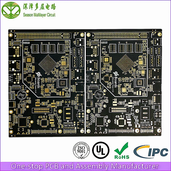
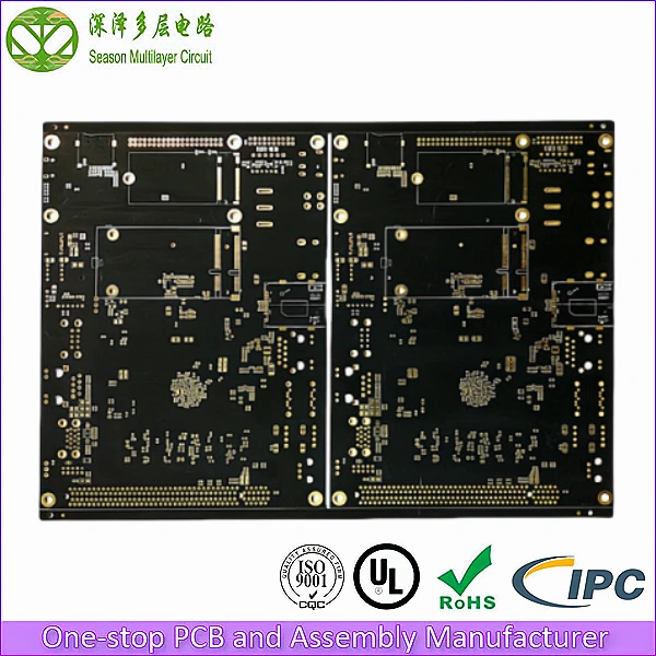
This 8-layer intelligent terminal PCB is a high-precision multilayer board engineered for next-generation smart devices. Designed around the RK3399 platform with 3/3mil trace/space, ENIG surface finish, and FR4 Tg 180 — delivering uncompromising signal integrity for tablets, POS terminals, self-service kiosks, and IoT edge devices.
As a specialized intelligent terminal PCB manufacturer, Season PCB supports everything from 5-piece prototypes to 100,000+ piece production runs — with blind/buried vias, 0.20mm min drilling, and TDR-verified impedance control on every panel. Need boards fast? Explore our fast PCB manufacturing services for quick-turn options.
✓ ±10% Impedance Control — Polar TDR verified on every panel
✓ TDR Test Per Panel — full impedance coupon report included
✓ No MOQ — from 5-piece prototypes to 100,000+ volume
✓ 24h DFM Review — free engineering review of your Gerber files
✓ Turnkey PCBA — component sourcing and assembly under one roof
8
Layer Count
3/3 mil
Min. Trace / Space
0.20 mm
Min. Via Diameter
Tg 180
Glass Transition Temp
1 µ”
ENIG Gold Thickness
ISO 9001:2015
ISO 14001
UL (E305905)
IPC Class 2 / Class 3
IATF 16949
RoHS
8-Layer Intelligent Terminal PCB Stackup Diagram
For security hardware, signal integrity is everything. Our standard 8-layer stackup maximizes shielding by sandwiching high-speed routing layers between solid ground and power planes.
- L1 — Top Layer (Copper / Plated): Main SoC placement, high-speed differential pairs, DDR escape routing, fine-pitch BGA fan-out. Direct contact with ENIG surface finish for SMT assembly.
- L2 — Inner Ground Plane: Reference plane for L1 signals, provides clean DDR return path, assists top-layer heat dissipation toward internal thermal vias.
- L3 — Inner Signal Layer: High-speed signals — DDR CMD/CTRL, PCIe Gen 2/3, USB 3.0/3.1 differential pairs. Stripline routing between L2 and L4 reference planes.
- L4 — Inner Power Plane: Multiple power domains (VDD_CPU, VDD_GPU, VDD_CENTER, DDR_VDDQ). Low-impedance PDN with distributed decoupling capacitors on adjacent layers.
- L5 — Inner Ground Plane: Reference ground, EMI shielding between L4 power plane and L6 signal layer. Ensures crosstalk-free separation of power and secondary signal domains.
- L6 — Inner Signal Layer: eMMC/SDIO storage bus, HDMI 2.0, RGMII Ethernet, I2S audio, GPIO break-out. Lower-speed routing with relaxed impedance requirements.
- L7 — Inner Ground Plane: Reference plane for L6 & L8, bottom-side shielding, thermal copper pour for passive heat dissipation.
- L8 — Bottom Layer (Copper / Plated): Bottom-side components, decoupling capacitor array, test points, secondary low-speed signals, conformal coating area.
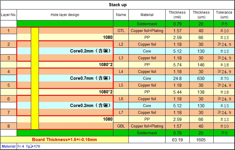
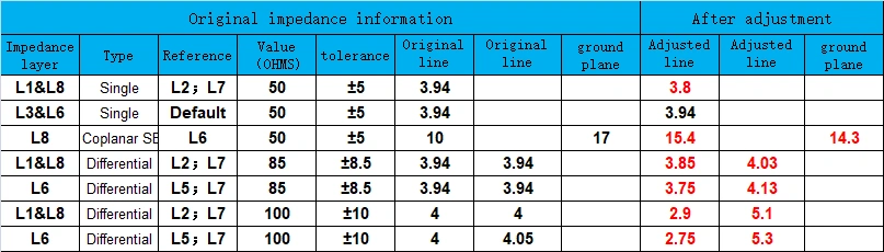
Custom stackup architectures available — our engineering team makes micro-adjustments to your trace dimensions to guarantee impedance performance.
Contact us for custom stackup design →
Every production panel includes dedicated impedance coupons tested via Time Domain Reflectometry (TDR), guaranteeing ±10% impedance control across single-ended (50Ω) and differential pairs (85Ω, 100Ω). Full TDR test reports ship with your order — no extra charge.
Technical Capability & Specifications
| Parameter | Specification | Advanced Capabilities |
|---|---|---|
| Layer Count | 8Layer | 2-32L(Mass); 2-64L(Sample) |
| Base Material | FR-4 S1000-2M Tg 180 | SY, NY,TUC,ZY,EMC,KB,ITEQ, Rogers, Megtron , Nelco,Isola |
| Board Thickness | 1.6mm | 0.2-6.4mm(Mass);0.15-20mm(Sample) |
| Panel Size | 242*170mm/2 | 800*600mm(Mass);1050*610(Sample) |
| Copper Thickness | Outer: 1 oz Inner: 1 oz | Outer: 1/3–12 oz Inner: 1/4–12 oz |
| Min Drill Size | 0.2mm | 0.15mm(Mass);0.127mm(Sample) |
| Min Trace Width/Spacing | 3/3mil | 2.36/2.36mil(1 oz) 2/2mil(0.5 oz) |
| Min BGA Pad | 0.25mm | 0.15mm |
| Surface Finish | ENIG 1 µ” | OSP,ENIG,HASL,Electric Hard Gold, ENIG+OSP,ENEPIG,Immersion Silver & Tin |
| Solder Mask Color | Matte Black | Green, Blue,Black,White,Yellow,Red,Purple, Matte Green,Matte Blue,Matte Black |
| Impedance Control | ±10% (50/85/100Ω) | ±5% (Strict Tolerance) |
| Min Routing Tolerance | ±0.15mm | ±0.075mm |
| Quality Standard | IPC Class 2,RoHS | IPC Class 3, UL, RoHS,IATF 16949,GJB |
| PCB Type | Multilayer | HDI,Multilayer,Rigid-Flex,High Frequency,High Speed,Hybrids & Mixed Dielectrics |
Why Your Intelligent Terminal Needs an 8-Layer PCB
Modern intelligent terminals — from RK3399-powered Android tablets to Snapdragon-based AR headsets — pack multi-core application processors, high-bandwidth DDR3/DDR4 memory, gigabit Ethernet, and multiple wireless radios onto a single PCB. Only an 8-layer stack-up provides the plane structure, routing density, and impedance control these platforms demand. Below are the four engineering reasons why.
🔋
Superior Power Delivery Network (PDN)
Dedicated power and ground planes reduce power supply impedance dramatically. This ensures rock-stable voltage rails even under instantaneous surge currents — critical for multi-core application processors (RK3399, Snapdragon, MTK Dimensity) that draw heavy transient loads during boot bursts and peak compute workloads.
📶
Excellent Signal Integrity & EMI Control
Embedded stripline routing between continuous reference planes delivers precise ±10% differential impedance for USB 3.0, HDMI 2.0, PCIe Gen 2/3, and DDR3/DDR4 interfaces. Internal ground planes suppress crosstalk between adjacent high-frequency lanes and reduce radiated EMI below CISPR 32 Class B limits.
🌡️
Thermal Management & High-Tg Reliability
Built on FR4 S1000-2M Tg 180 laminate, the board withstands lead-free reflow temperatures up to 260°C. Inner 1 oz copper planes function as integrated heat spreaders, pulling heat away from SoC hotspots for long-term operational stability under sustained 24/7 loads.
⚡
Strict Analog-Digital Partitioning
Dedicated internal layers allow clean isolation between sensitive analog circuitry (GPS L1/L5, Wi-Fi 6, Bluetooth LE, audio CODEC) and high-speed digital logic. This prevents digital switching noise from contaminating weak analog signals, preserving receiver sensitivity and audio SNR.
Core Application Scenarios
The 8-layer intelligent terminal PCB is the backbone of a wide range of smart devices where high-speed processing, connectivity, and reliability converge. Below are the primary verticals where our boards are deployed in volume production today.
📱
Mobile Communication Devices
Smartphones, tablets, and video conferencing endpoints running 4G/5G and Wi-Fi 6. Clean RF-to-digital isolation eliminates dropouts and reduces packet loss in real-time HD calls.
🎮
Digital Entertainment & Gaming
Handheld game consoles, streaming media players, and VR/AR headsets. Ultra-low PDN impedance keeps frame rates smooth and latency imperceptible during GPU-heavy rendering.
💼
Mobile Office & Productivity
Vehicle-mounted navigation, handheld GPS/GNSS terminals, and surveying equipment. Analog-digital partitioning preserves nanovolt-level signal purity for sub-meter satellite positioning.
🗺️
Smart Navigation & Positioning
Ticket vending machines, ATM kiosks, POS terminals, and government self-service systems powered by RK3399 SoCs. Turnkey PCB and PCBA solutions for 24/7 public-facing equipment.
🏧
Self-Service Kiosks & POS
Ticket vending machines, ATM kiosks, POS terminals, and government self-service systems powered by RK3399 SoCs. Turnkey PCB and PCBA solutions for 24/7 public-facing equipment.
🌐
IoT Edge & AI Terminals
Edge AI inference boxes, smart speakers with on-device voice processing, and industrial IoT gateways. Low-Df materials and HDI via structures support high-bandwidth NPU-to-DDR interconnects.
Layer Stack-Up Comparison: 4L vs 6L vs 8L
| Feature | 4-Layer / 6-Layer PCB | 8-Layer PCB (Our Solution) |
|---|---|---|
| Routing Space | Limited — 2 or 3 signal layers; BGA fan-out is tight | Abundant — 4+ signal layers; effortless BGA escape routing |
| EMI Shielding | Weak — insufficient continuous ground references | Excellent — every signal layer has an adjacent reference plane |
| PDN Impedance | High — increased voltage ripple under load | Ultra-low — dedicated power/ground plane pairs |
| Impedance Control | ±10% or worse | ±10% — meets USB 3.0 / HDMI / PCIe standards |
| Crosstalk | Noticeable in high-speed designs | Minimized through stripline routing and shielding |
| Thermal Performance | Marginal — smaller copper area for heat sinking | Superior — thick internal copper planes act as heat spreaders |
| Suggested Use | Simple consumer electronics, low-speed I/O | Tablets, POS machines, IoT gateways, edge AI devices |
Key Manufacturing Process Capabilities
Producing a reliable 8-layer intelligent terminal PCB requires equipment and processes far beyond standard 2-layer boards. Our factory floor integrates the following technologies to guarantee registration accuracy, plating uniformity, and electrical integrity on every panel.
- Laser Direct Imaging (LDI) — sub-mil registration accuracy for 3/3 mil trace/space
- Vacuum Lamination Press — eliminates voids and guarantees uniform dielectric thickness
- Pulse Plating — achieves uniform copper distribution inside high-aspect-ratio microvias
- Automated Optical Inspection (AOI) — 100% inspection on all layers, flagging opens/shorts before lamination
- Flying Probe & Fixture Electrical Test — every board tested; no escapes
- Cross-Section Analysis — destructive physical analysis performed per lot to verify plating thickness and registration
- Impedance TDR Testing — time-domain reflectometry coupons built into every panel; guaranteed ±10%
Full Ecosystem Chipset Compatibility
Our 8-layer intelligent terminal PCBs have been validated across the major ARM SoC platforms powering today’s smart devices. We bring deep design-for-manufacturing (DFM) experience to each platform, helping you avoid common layout pitfalls before they become field failures.
Rockchip RK3399 / RK3588
Reference platforms for Android tablets, kiosks, and digital signage. We have extensive experience with RK3399 8-layer HDI designs — DDR3/DDR4 routing, USB 3.0, and HDMI 2.0 impedance verified on every build.
Qualcomm Snapdragon
High-performance smartphone and VR headset platforms. Our blind/buried via process reliably escapes 0.4 mm-pitch Snapdragon BGA packages and routes dense DRAM interfaces with tight impedance margins.
MTK Dimensity & Kompanio
Cost-optimized tablet and Chromebook SoCs. Our 8-layer stack-up provides cost-effective yet electrically robust PDN designs that help customers achieve competitive BOM costs without sacrificing signal integrity.
Allwinner & Amlogic
Set-top box and AIoT gateway platforms. Optimized low-speed and mixed-signal routing with strict analog isolation for Wi-Fi / BT coexistence — proven in millions of deployed units.
Quality Assurance & Certifications
In the intelligent terminal industry, even a 0.1% defect rate can translate into thousands of field failures. We enforce a zero-defect culture with multi-layered quality gates.
IPC-A-600 Class 2 / Class 3
All boards are manufactured and inspected to IPC standards. Class 3 (High-Reliability Electronics) available for mission-critical applications — tighter annular ring requirements, void-free plating, and stricter cosmetic criteria.
ISO 9001:2015 Certified
Our quality management system is certified by internationally accredited bodies. Full production lot traceability — from laminate batch number through to the final shipping label.
RoHS & REACH Compliant
All materials and processes comply with the latest EU RoHS Directive and REACH SVHC candidate list. We provide third-party lab test reports and compliance declarations with every shipment.
UL Recognized (E-305905)
Our PCB products carry UL recognition. This is essential for products destined for the North American market and is often a prerequisite for end-product safety certification. For the Canadian market specifically, our guide to cUL certified PCB requirements explains what the extra recognition covers.
Season PCB is your trusted partner for intelligent terminal PCB manufacturing. Our intelligent terminal PCB solutions support RK3399 and similar platforms with high-density routing and precise impedance control. Each intelligent terminal PCB is manufactured to IPC Class 2 or 3 standards.
For reliable intelligent terminal PCB production, Season PCB offers fast turnaround and no MOQ. Contact us today for your intelligent terminal PCB manufacturing requirements.
As a leading manufacturer of intelligent terminal PCB boards, Season PCB delivers reliable solutions for smart home, retail, and industrial IoT applications. Our intelligent terminal PCB production meets strict quality standards with full electrical testing and AOI inspection on every board.
Our intelligent terminal PCB designs follow IEEE connectivity standards and IPC manufacturing specifications. Each intelligent terminal PCB is tested for signal integrity and thermal performance. Volume programmes of this build run on 998PCB Group’s 2–30 layer PCB lines under the same quality system.
Frequently Asked Questions
Why do modern intelligent terminals prefer 8-layer PCBs over cheaper 4-layer or 6-layer alternatives?
Modern smart terminals integrate high-speed CPUs, DDR memory, and Wi-Fi/5G radios on a single board — resulting in extreme component density. An 8-layer PCB provides independent power and ground planes that form a natural electromagnetic shield. This enables precise impedance control on high-speed signal traces, suppresses crosstalk between adjacent high-frequency lanes, and dramatically lowers radiated EMI. The net effect is stable, glitch-free operation during HD video conferencing, gaming, or multi-radio data transfers — something 4- and 6-layer boards simply cannot guarantee.
Can SeasonPCB support controlled impedance on my 8-layer design, and what tolerance do you guarantee?
Absolutely. We offer ±10% impedance control across single-ended (50Ω) and differential pairs (90Ω, 100Ω) as standard. Each production panel includes a dedicated impedance coupon that is tested via TDR (Time Domain Reflectometry). The test data is included in your shipment report. If your design requires tighter tolerance, let us discuss it during DFM review.
What is the minimum order quantity (MOQ) and typical lead time for 8-layer intelligent terminal PCBs?
For rapid prototyping, we accept as few as 5 pieces with a turnaround time of 5–7 working days (depending on stack-up complexity). For volume production, typical lead time ranges from 2–4 weeks. We also offer an expedited service for urgent projects. Contact our sales team with your Gerber files for an exact quotation and delivery schedule.
Which chipset platforms have you validated for 8-layer intelligent terminal PCBs?
Our 8-layer intelligent terminal PCBs are validated across the major ARM SoC platforms: Rockchip RK3399 / RK3588 for Android tablets, kiosks and digital signage (DDR3/DDR4 routing, USB 3.0 and HDMI 2.0 impedance verified on every build); Qualcomm Snapdragon, where our blind/buried via process escapes 0.4 mm-pitch BGA packages and routes dense DRAM interfaces with tight impedance margins; MTK Dimensity and Kompanio for cost-effective PDN designs on tablets and Chromebooks; and Allwinner / Amlogic set-top and AIoT gateway platforms with strict analog isolation for Wi-Fi / BT coexistence, proven in millions of deployed units.
What manufacturing processes guarantee quality on your 8-layer intelligent terminal PCBs?
Every panel is built with Laser Direct Imaging for sub-mil registration accuracy on 3/3 mil trace and space, vacuum lamination for void-free uniform dielectric thickness, and pulse plating for uniform copper distribution inside high-aspect-ratio microvias. Quality is enforced by 100% automated optical inspection on all layers, flying probe and fixture electrical test on every board, cross-section analysis performed per lot, and impedance TDR testing coupons built into every panel with a guaranteed ±10% tolerance.
Ready to Build Your Next Intelligent Terminal?
Upload your Gerber files and get an engineered DFM review within 24 hours. No minimum order. Free file checking. Competitive pricing.
Tel: (+86) 18681528532 (WhatsApp)
E-mail: roc@season-pcb.com