Book Appointment Now

What drives PCB cost per square meter and how to read a quote: layer count, material and finish factors, panel utilization, and prototype vs volume pricing.
PCB Cost per Square Meter: How Quotes Are Built and Compared
Ask five suppliers what a board costs and you will often get five numbers spread across a factor of three, all of them technically correct. The reason is that PCB cost per square meter is a billing unit, not a single price: the same double-sided design can sit anywhere inside a wide band once material grade, surface finish, copper weight and quantity are varied. Treating the per-area number as the answer, rather than as the unit the answer is expressed in, is where most quoting arguments start.
This article shows how a per-area quotation is actually assembled. It gives a relative baseline by layer count, breaks down the five factors that multiply on top of it, explains the panel-utilization gap between net board area and billed area, and separates prototype economics from volume economics. It closes with a parameter-alignment checklist for comparing two quotes that disagree, so the comparison lands on facts instead of on gut feeling.
Table of Contents
- What PCB Cost per Square Meter Actually Measures
- Baseline Cost by Layer Count
- The Quote Formula: Base Price Times Five Factors
- From Price per Square Meter to Price per Board: Panel Utilization
- Prototype vs Volume: Why Unit Prices Fall With Quantity
- Market Factors Moving Prices in 2026
- How the Cost Logic Shifts by Board Type
- How to Compare Two Quotes That Disagree by a Factor of Three
- How to Get an Accurate PCB Cost per Square Meter Quote
- Frequently Asked Questions About PCB Cost per Square Meter
- Have the Stackup Reviewed Before You Compare Prices
What PCB Cost per Square Meter Actually Measures
A per-area figure answers a narrower question than most buyers intend. It describes what a fabricator charges for producing one square meter of finished panel under a specific process assumption, usually conventional glass-epoxy material, HASL finish, 1 oz copper and standard trace geometry. Change any of those assumptions and the same physical square meter is re-priced, because the factory is charging for process content, not for area alone.
This is why the question gets deflected so often. An honest answer requires the layer count, the material class, the finish, the copper weight and the quantity before it can be more than a range. A supplier who quotes a firm number immediately is either assuming a default recipe or leaving something out of it, and the buyer finds out which one only when the invoice arrives.
The useful reframe: treat the per-area unit as a measuring stick for comparing boards of different sizes within the same process family, and treat the factor breakdown in the next sections as the actual price. Both halves are needed to judge whether a quotation is reasonable.
Baseline Cost by Layer Count
Layer count is the largest single driver. Every additional layer pair adds inner-layer imaging, an extra lamination cycle, more drilling and more electrical test, and each of those steps consumes capacity and yield. The table below expresses typical layer-to-layer relationships as multipliers against a double-sided board built on conventional material, which is the closest thing the industry has to a baseline.
| Board type | Relative cost per square meter (double-sided baseline = 1.0) | Typical applications | Process difficulty |
|---|---|---|---|
| Single-sided | About 0.6 to 0.8 | Simple power supplies, LED lighting boards | Low |
| Double-sided | 1.0 (baseline) | Control boards, interface boards | Low |
| 4-layer | About 2.5 | Consumer electronics, industrial control | Medium |
| 6-layer | About 3.3 | Communication equipment, industrial mainboards | Medium |
| 8-layer | About 5 | Advanced industrial and medical equipment | High |
| 10-layer and above | 8 and upward | Servers, high-speed communication | High |
Read the multipliers as guidance for the conventional process window, not as a price list. Upgrading the material, changing the finish, thickening the copper or adding impedance control moves any row away from its baseline. The direction and rough size of those moves are exactly what the next table quantifies, and the final number is always confirmed at engineering review against the actual design data.
Two reference builds sit at different points of this ladder: a 4-layer SATA SSD board represents the common entry into multilayer territory, while an 8-layer security system board shows where lamination cycles and test coverage begin to dominate the arithmetic.
The Quote Formula: Base Price Times Five Factors
Underneath almost every quotation sits the same structure: a per-area base established by layer count, multiplied by a material factor, a surface-finish factor, a geometry and copper factor, a special-process factor, and a volume discount. Multipliers below are expressed against the conventional recipe, with the standard grade of glass-epoxy material and HASL finish set at 1.0.
| Quoting factor | Reference multiplier (standard recipe = 1.0) | What drives it |
|---|---|---|
| Material upgrade | Tg at or above 170 °C: about 1.1 to 1.3; halogen-free: about 1.2 to 1.5; low-loss high-speed grades: 2 to 5 | Resin system, certified supply and tighter processing windows |
| Surface finish | OSP: about 1.05 to 1.1; ENIG: about 1.15 to 1.3; plating higher still | Chemistry cost and line capacity |
| Copper weight | 2 oz: about 1.1 to 1.2; 3 oz and above: higher | Plating time and etch control on heavy copper |
| Trace and space | 4/4 mil: about 1.1 to 1.2; 3/3 mil: about 1.2 to 1.4 | Yield sensitivity of fine-line imaging |
| Special processes | Priced per item: impedance control, blind and buried vias, HDI by stage, resin plugging, edge plating | Each adds dedicated process steps outside the standard flow |
Two habits make this table usable. First, when comparing quotations, confirm that both sides are priced on the same recipe before comparing totals, because a factor-level difference explains most headline gaps. Second, treat the multipliers as orders of magnitude rather than commitments; the binding version of every factor is the one confirmed at engineering review, where the build is checked against the applicable IPC-6012 performance specification and the customer drawing.
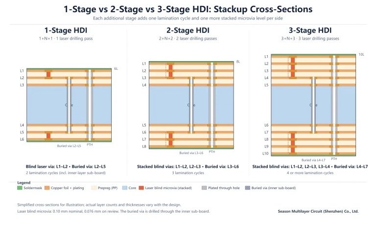
HDI deserves its own caution: the stage multiplier compounds. Each additional stage adds a laser pass and a lamination cycle, so a board quoted with two stages is not priced as a board with one stage plus a fixed surcharge, and the difference grows with every stage. The per-area unit survives, but the factor behind it moves the most here.
From Price per Square Meter to Price per Board: Panel Utilization
Fabricators bill production panel area, not the net area of the individual board. Boards are nested into manufacturing panels together with process rails and the gaps required for routing and depaneling, and typical utilization lands between 70% and 85%. Odd outlines and very small boards push utilization lower, which is why two boards with identical net area can carry different per-board prices.
A worked example makes the gap concrete. A 100 mm by 100 mm board has a net area of 0.01 m². Nested into a production panel at 80% utilization, the billed area for that board becomes 0.0125 m², a quarter again as much as the net figure. That difference is the cost of the scrap edge, and it is real manufacturing cost, not padding.
Three design-side actions reduce it directly:
- Keep board outlines close to standard panelization modules so nesting wastes less material.
- Plan process rails and board-to-board spacing once, early, instead of forcing a second panelization pass later.
- Order quantities in whole-panel multiples, so the last partial panel is not built at a structural disadvantage.
None of these actions change the design function; they change how much of the production panel the design consumes. On high-volume programs the difference between 70% and 85% utilization is one of the largest levers available without touching a single component.
Prototype vs Volume: Why Unit Prices Fall With Quantity
Every job carries a roughly fixed engineering cost that exists no matter how many boards are made: phototools, drill and routing programs, electrical test fixtures and the engineering review itself. Quantity determines how that fixed cost is divided, which is why the per-board price of five prototypes and the per-board price of five hundred boards are not related by a factor of one hundred.
| Order stage | Fixed engineering cost | Unit price level |
|---|---|---|
| Prototype (5 to 10 boards) | Carried entirely by the batch | Highest |
| Small batch (50 to 200 boards) | Partially amortized | Middle |
| Volume (1,000 boards and above) | Essentially diluted | Lowest |
As a planning figure, the same specification at volume typically reaches one third to one fifth of the prototype unit price. The per-area rate may barely move between the two stages; what changes is the amortization structure on top of it. This is also why per-area comparisons between a prototype house and a volume quote are misleading, because the two numbers describe different cost structures rather than different efficiency.
The practical consequence for planning: prototype expensively, but design the stackup as if it were going to volume, because material and process choices made at prototype stage are the ones that get carried forward. A line-by-line breakdown of what sits inside a finished-board price, including these fixed elements, is published in our components of PCB prices guide.
Market Factors Moving Prices in 2026
The first market variable this year sits in low-loss materials. Capacity expansions for higher-grade copper-clad laminate run on 18 to 24 month cycles, and scheduling for those grades remains tight, which keeps widening the premium between conventional and low-loss builds. Projects that specify low-loss material only where signal layers actually need it, rather than across the whole stack, are the ones that hold their budget.
The second variable is finish selection. ENIG carries a structurally higher factor than OSP, and that gap has been widening with input costs. For cost-sensitive projects without gold-finger or contact-pad requirements, it is worth asking the engineering team whether OSP substitution is acceptable for the assembly process in use, because the finish factor applies to every square meter produced.
The third variable is slower and more durable: equipment, copper foil and labor costs have been drifting upward together, which moves the whole price baseline gradually rather than in steps. For procurement, the useful response is not repeated spot comparison but framework pricing with one or two primary suppliers, which converts market drift into a managed variable instead of a recurring surprise.
How the Cost Logic Shifts by Board Type
Rigid multilayer boards follow the layer-count ladder from the baseline table, and the steps between rungs are worth internalizing. Moving from 4 layers to 6 adds two more lamination and inner-layer imaging cycles; moving from 6 to 8 adds more still, plus wider test coverage. Each step is a genuine process increment, which is why the multipliers grow faster than the layer count itself.
Flexible circuits break the rigid arithmetic entirely. Flex pricing combines area with layer count and point density, because the polyimide base material costs more than glass-epoxy and the yield is sensitive to batch and design geometry. A flex quote has to be reviewed against the actual circuit density, so per-area figures for flex are indicative in a way rigid-board figures are not.
Between those two families sit the hybrid builds, where a low-loss material is pressed together with conventional layers so that only the signal-critical portion of the stack carries the material premium. For products such as an optical module board, hybrids routinely deliver most of the electrical benefit at a fraction of the full low-loss cost.
How to Compare Two Quotes That Disagree by a Factor of Three
Start by aligning parameters, in this order: material grade, surface finish, copper weight, minimum trace and space, impedance requirements and via structure. Most headline gaps close at this step, because one quotation was priced on a conventional recipe and the other on an upgraded one, and neither supplier did anything wrong by quoting what was written in front of them.
If the gap survives full alignment, send identical Gerber data to both suppliers and ask for an itemized breakdown. A legitimate gap at that point usually traces to panel utilization, test coverage or batch size assumptions. A gap that survives itemization too deserves scrutiny in the other direction: check whether the cheaper quotation quietly reduced a specification, because a downgraded material grade or a thinner copper weight saves the supplier far more than it shows.
The comparison habit worth building is to normalize before judging: convert every quotation to the same recipe, the same quantity and the same billed-area assumption, and only then rank them. Suppliers differ on efficiency, but not usually by a factor of three on an identical, fully specified build.
How to Get an Accurate PCB Cost per Square Meter Quote
The shortest path to a firm number is complete input. Submit the design in Gerber RS-274-X format together with the layer count, material grade, surface finish, copper weight, minimum trace and space, impedance targets, quantity and required lead time. With those parameters stated, PCB cost per square meter stops being a range and becomes a line-item quotation, because every factor in the formula above has been pinned to a value.
If the design is still at concept stage and Gerber output does not exist yet, a partial path remains: provide the outline dimensions, layer count and target material class, and the engineering team returns a reference band that tightens as the design matures. Early figures are useful for budgeting precisely because their assumptions are stated, and they carry an explicit reminder that the binding version comes at review.
Standard lead-time windows by layer count and process, which belong in any RFQ alongside the price request, are summarized on our PCB lead time page.
Frequently Asked Questions About PCB Cost per Square Meter
What is a reasonable PCB cost per square meter?
It depends first on layer count and then on the process recipe built on top of it. A conventional double-sided board is the baseline, a 4-layer board runs roughly two and a half times that baseline, and the multiplier climbs from there with material upgrades, finish changes and special processes. The practical test of reasonableness is parameter alignment: confirm the recipe behind each quotation, then compare like for like. A figure far below the aligned band deserves a specification check before it deserves celebration.
How much more does a 4-layer board cost than a double-sided board?
Per square meter, a conventional 4-layer build typically lands around two and a half times the double-sided baseline, because two extra layers add inner-layer imaging, an additional lamination cycle and wider electrical test. The multiplier moves further with material upgrades, impedance control or blind and buried vias. It is a relative guide rather than a quotation, and the exact figure is confirmed at engineering review against the actual design data.
Why do two quotes for the same design differ by several times?
Because the per-area unit hides the recipe behind it. One quotation may assume a conventional material and finish while the other prices an upgraded grade and ENIG; one may assume 80% panel utilization where the other assumes 70%; one may include impedance control and special processes as line items while the other excludes them. Aligning material, finish, copper weight, trace geometry, via structure and quantity explains most gaps. Whatever remains after alignment should be resolved with an itemized breakdown based on identical Gerber data.
Why is prototype pricing higher per board than volume pricing?
Every job carries fixed engineering costs, including phototools, drill and test programs and the engineering review, which exist regardless of quantity. On a five-board prototype those costs are carried entirely by the batch; at volume they are diluted across thousands of boards. The same specification at volume typically reaches one third to one fifth of the prototype unit price, even though the underlying per-area rate changes far less than the per-board total.
How does panel utilization affect what I pay?
Fabricators bill production panel area, and boards typically consume 70% to 85% of it once process rails and spacing are included. A 100 mm by 100 mm board nested at 80% utilization is billed on 0.0125 m² instead of its 0.01 m² net area. Outlines that nest efficiently, rails planned once up front and quantities ordered in panel multiples all push utilization upward, which is one of the few cost levers that costs the design nothing.
Is a flexible circuit priced the same way as a rigid board?
No. Flex pricing combines area with layer count and circuit point density, because the polyimide base material costs more than glass-epoxy and yield is sensitive to both batch size and design geometry. Per-area figures for flex are therefore indicative only, and a meaningful number requires the actual circuit layout and density to be reviewed. Rigid-flex constructions are quoted as their own category, since they combine both process chains.
What should I include in an RFQ to get an exact price?
Submit the Gerber data together with layer count, material grade, surface finish, copper weight, minimum trace and space, impedance targets, quantity and required lead time. Each of those parameters corresponds to a factor in the quoting formula, so stating them converts the answer from a range into a line-item quotation. Complete input also lets the engineering team flag any parameter that will fight the process, which is cheaper to learn before tooling than after.
Have the Stackup Reviewed Before You Compare Prices
Send the Gerber data with layer count, material grade, surface finish, copper weight, impedance targets, quantity and lead time. The engineering team returns an itemized quotation that shows the base and every factor on top of it, so the comparison against any other quotation happens on aligned parameters instead of on headlines.
The review is part of our PCB manufacturing service, from first prototypes through production volumes, and it is also where panelization and material substitutions that reduce the per-area figure without touching performance usually get found.