Book Appointment Now

Why PCB crosstalk appears at corner rather than in layout review: coupling paths, 3W spacing limits, reference plane continuity and a bring-up checklist.
PCB Crosstalk: Causes, Spacing Rules and Fixes
PCB crosstalk is the failure mode that survives schematic review, passes layout review and then appears as a bit error on the bench at the worst possible moment. It is not a mysterious effect: it is capacitive and inductive coupling between conductors that share the same dielectric space, and it scales with how close those conductors are relative to how thin the dielectric is. That single ratio explains most of what designers argue about.
This guide works through the coupling paths, what spacing rules actually guarantee, which stackup decisions set the baseline before any routing starts, and which fabrication controls protect the margin you designed. It is written for the point where a design is about to be released or a prototype is failing, so each section ends in something you can check rather than something you can admire.
Table of Contents
- What PCB Crosstalk Is and Why It Shows Up Late
- The Three PCB Crosstalk Coupling Paths Engineers Debug
- Reading the Coupling Ratio Without a Field Solver
- Spacing Rules: 3W, 4W and When They Are Wrong
- Reference Plane Continuity and the Return Path
- Stackup Decisions That Set the Baseline
- Differential Pairs, Guard Traces and Shielding
- Manufacturing Controls That Protect the Margin
- A Bring-Up Checklist for Suspected Crosstalk
- When to Bring the Fabricator In Early
- FAQ
- Send the Stackup Before the Layout Freezes
What PCB Crosstalk Is and Why It Shows Up Late
When a signal switches, the field between the trace and its reference plane has to be rebuilt. A neighbouring trace sitting in part of that field sees a fraction of the transition, in the form of a current injected through mutual capacitance and a voltage induced through mutual inductance. PCB crosstalk is the sum of those two contributions appearing on a line that was supposed to be quiet.
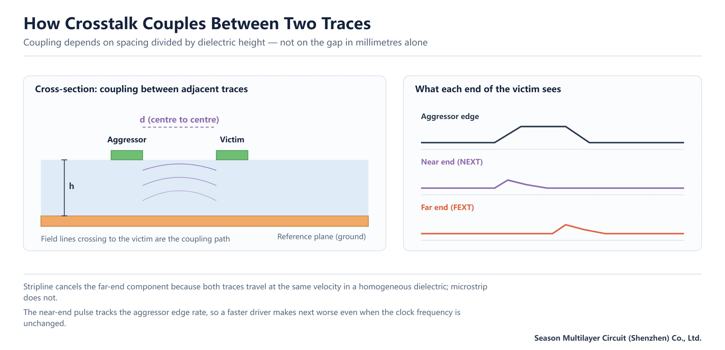
The two ends of the victim trace receive different things. At the end nearest the driver you get near-end crosstalk, which is the sum of the coupled contributions arriving back towards the source; at the far end you get far-end crosstalk, which depends on the difference in propagation between the two lines. In stripline, where both traces sit between planes and travel at the same velocity, far-end crosstalk largely cancels. In microstrip it does not, which is why surface routing is the usual suspect.
The reason it shows up late is that coupling is a threshold effect. A layout can be 20% over the comfortable limit and still pass every functional test at room temperature, then fail when a link negotiates at a higher rate, when a cable adds loss, or when the board runs hot and the driver slows down. Margin is consumed by everything else first, so crosstalk gets blamed last even when it was the largest single contributor.
The Three PCB Crosstalk Coupling Paths Engineers Debug
Almost every crosstalk investigation ends in one of three mechanisms, and separating them early saves days. The first is electric field coupling through mutual capacitance, dominant when a fast edge faces a quiet line across a thin dielectric at high impedance. It injects a narrow spike that follows the edge rate, so it gets worse as drivers get faster even when the clock stays the same.
The second is magnetic coupling through mutual inductance, which dominates on low-impedance nets such as power distribution and on wide traces carrying large di/dt. Its signature is a slower, wider disturbance that tracks the current loop rather than the voltage edge. The third is common impedance coupling: two circuits sharing a return path whose inductance cannot be ignored, so the switching current of one develops a voltage that the other sees as its own reference moving.
| Coupling path | Typical signature | Where it originates |
|---|---|---|
| Mutual capacitance | Narrow spike aligned with the aggressor edge | Thin dielectric, long parallel run, high-impedance victim |
| Mutual inductance | Wide disturbance following the current loop | Power distribution, wide traces, poor return path |
| Common impedance | Offset or bounce on a reference that two circuits share | Split planes, thin return traces, connector pin sharing |
In practice the three arrive together and the art is deciding which one to attack first. A useful test is to slow the aggressor edge without changing anything else: if the disturbance shrinks proportionally, capacitance is leading. If it barely moves, the current loop is the problem and no amount of spacing will rescue the design.
Reading the Coupling Ratio Without a Field Solver
Coupled noise on a microstrip pair falls off approximately with the square of the ratio between centre-to-centre spacing and dielectric height. In plain terms, the useful variable is not the gap in millimetres, it is the gap divided by the height to the reference plane. Doubling the spacing cuts the coupling to roughly a quarter; halving the dielectric height while keeping the spacing doubles the ratio and does the same thing from the other direction.
Two more factors matter and neither is visible in a spacing rule. Coupled length matters up to the point where the coupling saturates, which is roughly when the line length exceeds the edge’s electrical length. Rise time matters because a faster edge contains more energy at the frequencies where coupling is efficient; a 100 ps edge and a 500 ps edge on the same geometry are not the same design.
That is why copying a spacing number from another project goes wrong. The number came from a specific stackup with a specific dielectric height and a specific driver. If your board is thinner, the same spacing is worth less; if your edge is faster, the same spacing is worth less again. The ratio transfers, the millimetre figure does not. The generic routing guidance behind these rules sits in the IPC-2221 and IPC-2226 design standards, which describe the geometry that a constraint set is supposed to express.
Spacing Rules: 3W, 4W and When They Are Wrong
The industry shorthand is the 3W rule: keep centre-to-centre spacing at least three times the trace width. It is a reasonable starting point for microstrip at moderate edge rates and it is easy to check in a design rule. It is also frequently misapplied, because the letter W in the rule refers to trace width while the physics refers to dielectric height. On a thin board with wide traces the two diverge badly.
| Rule of thumb | What it assumes | When it is not enough |
|---|---|---|
| 3W centre-to-centre | Microstrip, dielectric height near trace width, edges slower than about 300 ps | Thin dielectric, wide traces, or long parallel runs on the same layer |
| 4W or more for clocks and resets | Sensitive or single-ended nets with no reference plane adjacency | Any net routed across a plane split, where the return path matters more than spacing |
| Double spacing on outer layers only | Stripline cancels far-end coupling by construction | Microstrip with fast edges, where far-end crosstalk does not cancel |
| Guard trace between aggressor and victim | The guard is stitched to the reference plane at intervals shorter than a tenth of the edge length | An unstitched guard trace, which behaves like a third coupled line |
The most common failure in practice is a guard trace that floats. An unstitched trace between two signals adds a conductor that couples to both, and at some lengths it makes the coupling worse rather than better. If a guard is used, it needs vias to the reference plane at regular intervals, and it needs to be wide enough that its own impedance is low compared with the coupling path.
A second failure is applying a spacing rule to the wrong layer stack. A stripline layer with 0.1 mm dielectric and 0.1 mm traces has a very different coupling environment from a 0.2 mm outer-layer microstrip, yet both may show the same 3W number in the constraint manager. Constraint values should be entered per layer class, not globally.
Reference Plane Continuity and the Return Path
Every signal returns to its source. On a well-built board it returns through the plane directly beneath the trace, following the path of least impedance, which at high frequency means least inductance. Cut that plane, or force the return current to cross a gap, and the current detours around the split, forming a loop that couples into anything nearby. This mechanism produces crosstalk between traces that are nowhere near each other on the same layer.
The rule that follows is simple to state and hard to hold: a high-speed net should never cross a plane split. When a net has to change reference layers, it needs a return via next to the signal via, so the return current can follow. Without it, the transition becomes a radiator, and the noise lands on whatever shares the new reference.
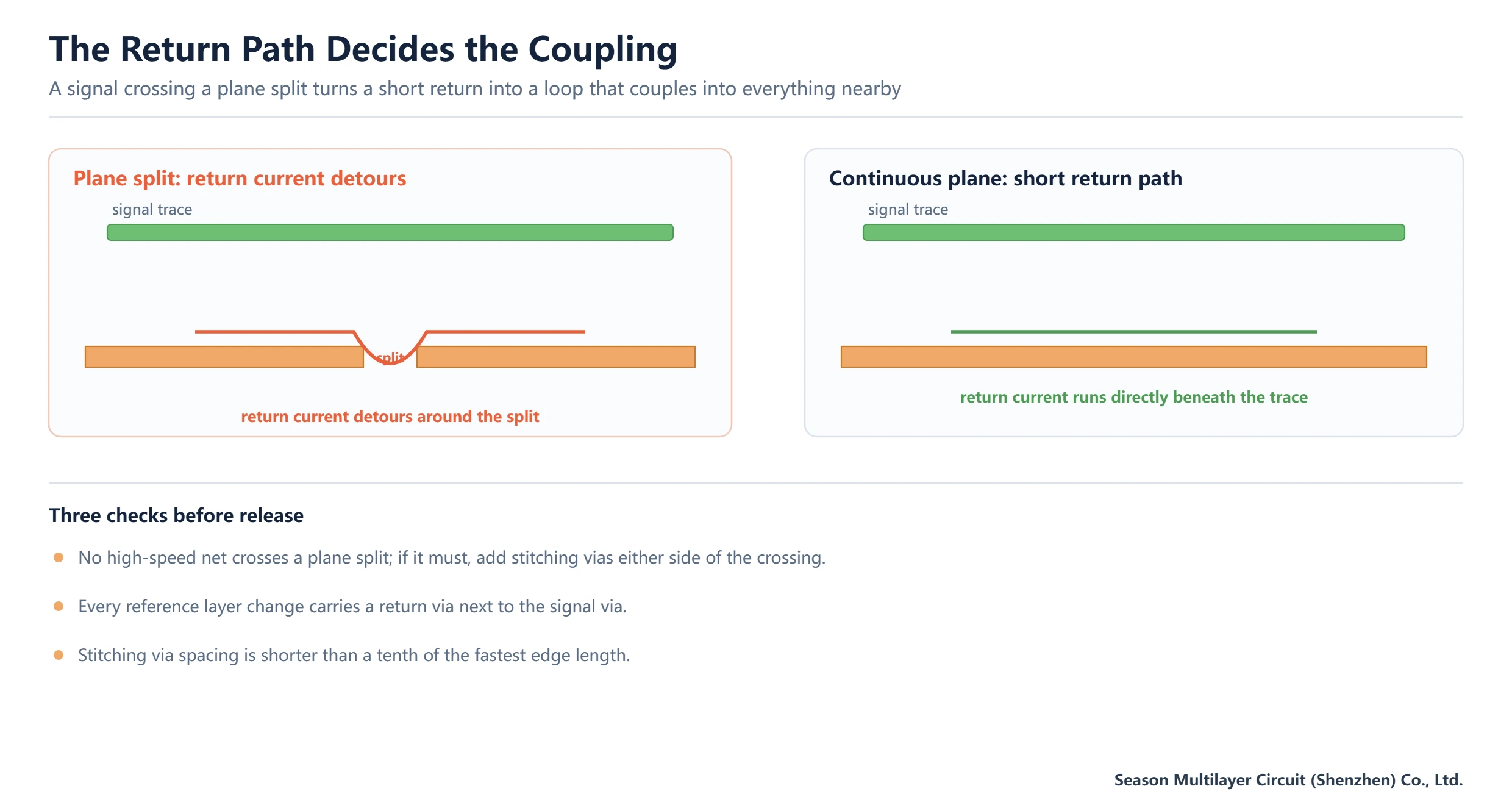
Power and ground plane pairs deserve the same attention. Two nets referencing different planes at the same nominal potential will still couple if the planes are not stitched together at the transition point. Stitching via placement is therefore a layout task, not a cosmetic one, and it shows up directly in crosstalk measurements on the finished board. The layer-level rules are covered in our stackup design guide.
Stackup Decisions That Set the Baseline
Before a single trace is routed, the stackup has already decided how much crosstalk the design can tolerate. Three decisions dominate: whether high-speed routing is on stripline layers or outer layers, how thick the dielectric is between the routing layer and its reference, and whether two high-speed routing layers are placed adjacent to each other.
Stripline is the strongest lever. A trace buried between two planes has its field confined, and as noted above, far-end crosstalk cancels because both lines travel at the same velocity in the same homogeneous dielectric. Moving a critical bus from the outer layer to an inner layer frequently solves a coupling problem that no spacing change could fix, at the cost of an extra layer pair and two more lamination cycles.
Thinner dielectric between signal and reference tightens coupling to the plane and reduces coupling to neighbours, but it also narrows traces for a given impedance, which raises conductor loss. That trade is exactly where the material tier question meets the geometry question, and it is worth settling both at once rather than iterating. Boards we build from 2 to 30 layers give plenty of room to place critical buses on stripline layers with a dedicated reference.
Adjacent high-speed routing layers with no plane between them are the classic mistake. Broadside coupling between the two layers can exceed edge-to-edge coupling on a single layer, and it is invisible to a spacing check that only looks within a layer. If such an arrangement is unavoidable, route the two layers orthogonally so the coupled length stays short.
Differential Pairs, Guard Traces and Shielding
Differential routing helps, but not for the reason usually quoted. A tightly coupled pair is more immune to external noise because the disturbance appears as common mode and is rejected by the receiver. That immunity depends on symmetry: unequal trace lengths, asymmetric spacing or a reference plane that only sits under one leg will convert common-mode noise into differential noise, which is the part the receiver cannot reject.
Shielding works when it is grounded and complete, and disappoints when it is neither. A metal can over a radio section, a grounded fence along a board edge, or a stitched guard between an aggressor bus and a sensitive analogue block all reduce coupling meaningfully. A floating copper pour between two traces does not; it couples to both and re-radiates.
Filtering belongs in the same conversation. Series termination slows the edge and reduces the high-frequency content that drives capacitive coupling, which is why a 22 Ω to 33 Ω series resistor on a clock sometimes fixes a problem that spacing could not. Ferrite beads and common-mode chokes help at connector boundaries, where the coupling path leaves the board and the geometry is no longer under your control.
Manufacturing Controls That Protect the Margin
A design with 6 dB of PCB crosstalk margin can still fail if the fabricated geometry lands at the edge of tolerance. Two fabrication variables matter most: impedance control and etch compensation. If the dielectric thickness comes in at the low end and the trace etches narrow, impedance rises, coupling rises with it, and the margin quietly disappears.
We hold ±10% impedance as standard, tighten to ±8% and ±5% on request for dense high-speed work, and measure with TDR coupons from the same panel. That measurement is what makes a coupling calculation meaningful, because the model used the nominal Dk and the nominal height. The methods and coupon design are described in our impedance measurement guide.
The second control is laminate consistency. Dk varies by lot and by resin content, and a mid-loss grade specified at a nominal value will move a few hundredths between batches. On a design with tight spacing that shift changes both impedance and coupling. Recording the lot-level Dk on the material certificate, and re-checking first-article coupons when the supplier or the batch changes, is cheaper than a respin.
Layer registration belongs on the list too, especially on thick boards. If the reference plane shifts relative to the signal layer by more than the design allows, the effective dielectric height changes across the panel and coupling varies from board to board. Registration tolerance is a fabrication parameter that designers rarely ask about and that quietly sets the spread of a build. It only means anything if the Gerber data and the fabrication drawing carry the same layer stack and the same revision.
A Bring-Up Checklist for Suspected Crosstalk
When a prototype shows errors that look like noise, the fastest route is to establish whether the mechanism is really coupling before touching the layout. The table below maps the symptom to the most likely cause and the first measurement to take.
| Symptom | Most likely cause | First action |
|---|---|---|
| Errors only on one adjacent pair of nets | Edge-to-edge coupling on a parallel run | Measure the victim with the aggressor idle, then switching; compare amplitude |
| Errors appear when data rate rises but not when clock is steady | Far-end coupling on microstrip | Check whether the bus can move to a stripline layer in the next revision |
| Noise on many nets at once, worst near a connector | Common impedance or split plane crossing | Probe the reference plane at the connector; look for a plane cut under the bus |
| Disturbance follows a power event | Mutual inductance in the return path | Check stitching via density and plane pair assignment |
| Fails only at temperature or after hours of running | Margin consumed by drift, not by a single mechanism | Re-measure eye margin at corner; review impedance coupon data |
Two practical notes on measurement. A current probe on the aggressor is more informative than a voltage probe on the victim, because it shows the loop that is doing the coupling. And a near-field scan, even a crude one made with a loop of wire and a spectrum analyser, localises the coupling far faster than reasoning from the schematic.
When to Bring the Fabricator In Early
Crosstalk is usually treated as a design problem, but half of the available margin sits in fabrication. Impedance tolerance, dielectric thickness control, registration and material consistency all decide whether the coupling you calculated is the coupling you get. Bringing the fabricator in at stackup review, rather than at quotation, is the cheapest way to buy margin.
What to send is short: the stackup with target impedance per layer, the longest parallel run and its spacing, the edge rate of the fastest driver, and any nets that cannot be re-routed. With those, a fabrication engineer can tell you whether the dielectric heights in the drawing are buildable at the tolerance you need, and whether a different glass style would give a better height-to-spacing ratio. Our signal trace design rules summarise the constraint set we usually review against.
For dense designs the conversation usually lands on the same options: move the bus to stripline, thin the dielectric and accept narrower traces, or add spacing and lose routing density. Those are trade decisions with cost attached, and they are much cheaper to make on a drawing than on a second prototype. 10-layer 2-stage HDI builds and 14-layer computing boards are where we see this most often, because routing density and layer count are both near their limits.
Frequently Asked Questions
What causes PCB crosstalk?
Three mechanisms cover almost every case: mutual capacitance between traces sharing a dielectric, mutual inductance between current loops, and common impedance in a shared return path. The first dominates on fast edges across thin dielectrics, the second on power distribution and wide traces, and the third wherever a signal crosses a plane split. Most real failures are a combination, which is why fixing spacing alone sometimes changes nothing.
What is the 3W rule and is it enough?
The 3W rule keeps centre-to-centre spacing at three times the trace width, which limits coupling on microstrip at moderate edge rates. It is a starting constraint, not a guarantee. The physics depends on the ratio of spacing to dielectric height, so on a thin stackup with wide traces 3W can be inadequate, and on stripline layers the far-end component cancels anyway. Enter the value per layer class, not globally.
What is the difference between near-end and far-end crosstalk?
Near-end crosstalk appears at the end of the victim line closest to the aggressor driver and is the sum of the coupled contributions travelling back towards the source. Far-end crosstalk appears at the opposite end and depends on the difference in propagation velocity between the two lines. In stripline both lines travel in the same homogeneous dielectric, so the far-end component largely cancels; in microstrip it does not.
Does a guard trace reduce crosstalk?
Only if it is stitched to the reference plane at intervals shorter than about a tenth of the edge length. A floating copper trace between two signals behaves like a third coupled line and can make coupling worse at some lengths. When stitched properly and made wide enough to present a low impedance, a guard is effective, but it costs routing space that spacing would often use more efficiently.
Can a PCB manufacturer fix crosstalk on an existing design?
Not the routing, but the fabrication variables that decide whether the design’s margin survives. Impedance tolerance of ±10% as standard, or ±8% and ±5% on request, dielectric thickness control, layer registration and laminate Dk consistency all affect coupling. If those are held, the coupling you calculated is close to what the board delivers. If they drift, a passing design can measure badly.
How do I reduce crosstalk without adding layers?
Increase spacing on the parallel run, shorten the coupled length, slow the aggressor edge with series termination, and check that the return path under the victim is continuous. Moving to a thinner dielectric helps only if the trace geometry stays stable. If the bus is on an outer layer and the error is far-end coupling, adding a ground plane above it converts the geometry to stripline without adding a signal layer.
Why does crosstalk only appear at high temperature?
Temperature rarely creates coupling; it consumes the margin that was hiding it. Driver edge rates slow, dielectric loss rises, resistance rises and timing shifts, so a link that passed at room temperature with 2 dB of margin can fail at the corner. If the failure is thermal, treat the coupling budget as a margin problem rather than a defect and re-measure eye height at temperature.
Send the Stackup Before the Layout Freezes
Coupling margin is cheapest to buy on a drawing. Send the stackup with target impedance per layer, the longest parallel run, and the fastest edge rate in the design, and we will confirm whether the dielectric heights are buildable at the tolerance your coupling budget assumes.
The review covers impedance control, glass style and dielectric height options, registration tolerance and the coupon plan for verification. Start with a stackup review request, or read the wider HDI technology guide if the design is moving to finer geometry.