Book Appointment Now

How one 16-layer 2-stage HDI PCB moved from 1 oz copper on every layer to 0.5 oz inner layers, and the CAM checks that decide it before a panel is cut.
16-Layer 2-Stage HDI PCB: What a CAM Review Changes Before Production
A 16-layer 2-stage HDI PCB rarely fails because of one wrong number. It fails because the stackup, the copper weights and the impedance targets were each decided on their own and only met each other on the shop floor. What follows is the walkthrough of one such build – a high-performance SoC core board for an industrial vision and edge-compute device – and of the decisions the CAM review changed before a single panel was cut.
The design arrived as 16 layers, 2-stage HDI, 1 oz copper on every layer. It was released with 1 oz on the outer layers and 0.5 oz on the inner layers, with trace widths and spacings retuned against the pressed dielectric. Nothing about the board outline, the BGA or the layer count changed. Two process variables moved, and the impedance targets became achievable. This article explains why those two moved, and gives you the checklist for having that conversation before your own design reaches the factory.
Table of Contents
- Why a High Layer Count Board Gets Reviewed Before a Panel Is Cut
- What 2-Stage HDI Means on a 16-Layer 2-Stage HDI PCB
- Reading the Stackup: Layer Roles and Copper Weights
- Copper Weight vs Impedance on a 16-Layer 2-Stage HDI PCB
- Retuning Trace Width and Spacing Against the Pressed Stack
- Laminate Choice: What the Material Has to Survive
- Laser Microvias, Buried Vias and the Through Holes That Remain
- First-Article Confirmation and In-Process Inspection
- Cost and Lead Time: Where the Multipliers Come From
- Checklist Before You Release a 16-Layer 2-Stage HDI PCB
- FAQ
- Have Your Stackup Reviewed Before the Numbers Are Fixed
Why a High Layer Count Board Gets Reviewed Before a Panel Is Cut
CAM review is the point where a design meets a specific process. The data is checked against what the equipment can actually hold: drill-to-copper clearance, annular ring after drilling and plating, etch compensation, solder mask and legend clearances, press fit between copper-filled areas, panel utilisation, and whether the impedance targets are reachable on the stack as drawn. On a simple four-layer board most of these checks pass silently. On a 16-layer build they are the whole job.
The reason is compounding. A 16-layer 2-stage HDI PCB goes through the press more than once, and every cycle adds its own registration budget, its own plating thickness and its own imaging tolerance. An error that would be invisible on one cycle becomes a drill that misses its pad on the third. The same change that costs nothing at CAM costs a scrap panel after the first press.
There is also a habit worth breaking: the drawing is not the board. Nominal dielectric heights on a drawing describe the material before it flows. The impedance your signals see comes from the pressed height, which depends on how much copper is on the neighbouring layers and how the prepreg fills around it. Any review that treats the drawing as final will be surprised later.
What 2-Stage HDI Means on a 16-Layer 2-Stage HDI PCB
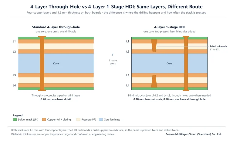
A stage is one build-up cycle of laser drilling, plating and imaging added to a face of the board. One stage gives you a single microvia layer on the outside; two stages give you two, usually stacked, so a signal can step from L1 to L2 and on to L3; three stages adds a third. Any-layer builds go further and place a microvia between any pair of adjacent layers. The count of stages is a process count, not a marketing label, and it maps directly onto how many times the panel is pressed and drilled.
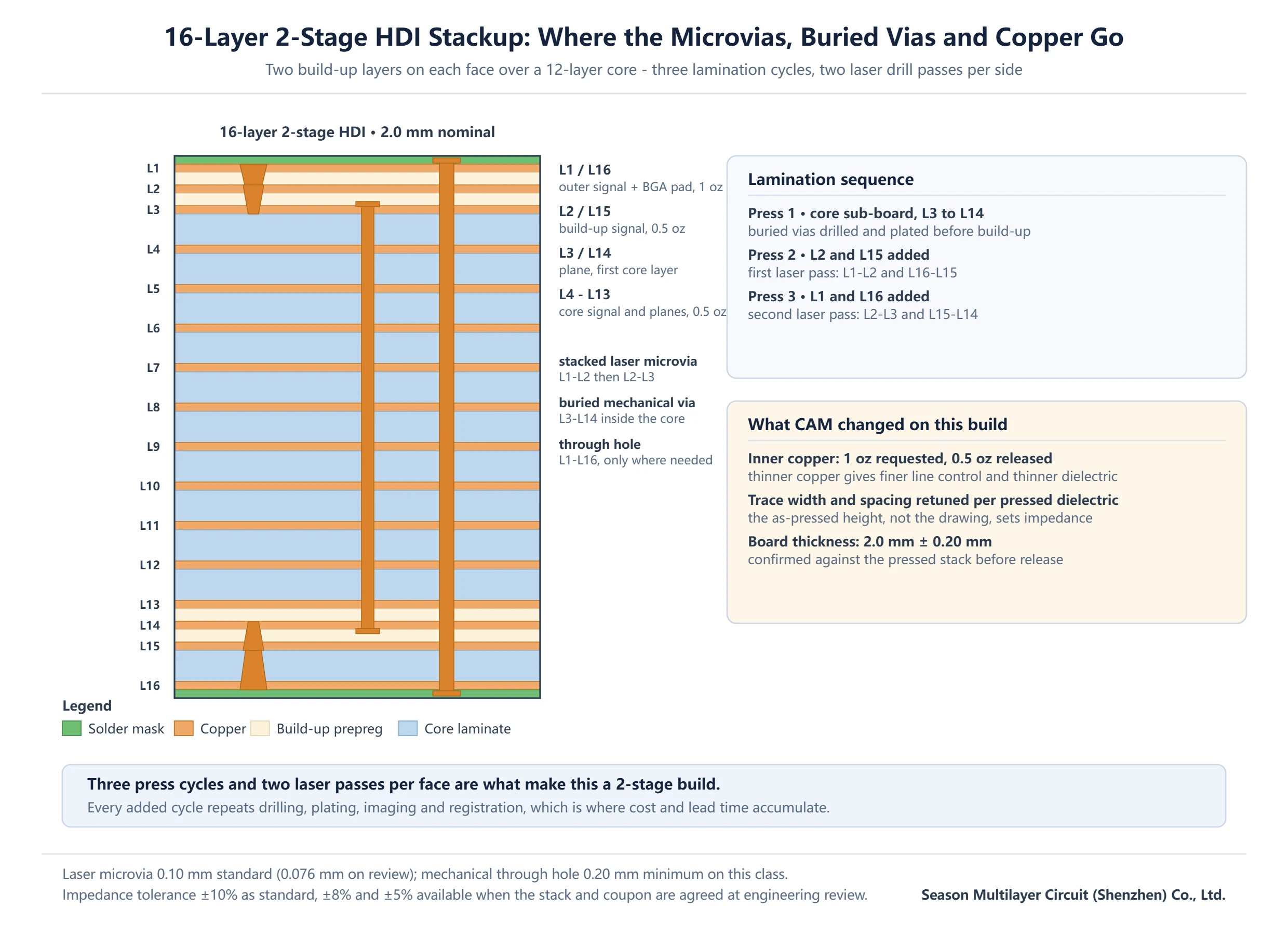
On this 16-layer 2-stage HDI PCB the core sub-board carries L3 through L14 with buried mechanical vias drilled and plated before any build-up starts. The outer faces are then built up twice: the first build-up adds L2 and L15 with a laser pass for L1-L2 and L16-L15, the second adds L1 and L16 with a second laser pass for L2-L3 and L15-L14. Through holes survive where they still earn their place – power, grounds, connectors, mounting.
The practical difference against a plain 16-layer through-hole board is routing freedom. Through holes consume a pad and a clearance hole on every layer they pass; microvias consume only the layers they connect. Under a fine-pitch BGA that difference decides whether you can break out the part at all. Our HDI PCB technology guide covers the structure rules, and the comparison of 1-stage, 2-stage and 3-stage HDI shows where each one stops paying for itself.
Reading the Stackup: Layer Roles and Copper Weights
Before any number is changed, the review assigns each layer a job. Outer layers carry the component pads and the BGA breakout, and they take the assembly and rework heat, so they keep the heavier copper. Inner signal layers are etched fine and carry less current, so they can go thinner. Plane layers are mostly solid copper, where weight is about current capacity and total thickness rather than etch resolution.
| Layer group | Role on this build | Released copper |
|---|---|---|
| L1 / L16 | Outer signal, BGA pads, microvia capture pads | 1 oz (35 µm) |
| L2 / L15 | Build-up signal, second-stage microvia landing | 0.5 oz (18 µm) |
| L3 / L14 | Reference planes, boundary of the core sub-board | 0.5 oz (18 µm) |
| L4 – L13 | Core signal pairs and plane pairs, buried vias | 0.5 oz (18 µm) |
Two things in that table are worth internalising. First, copper weight is not a single board-level setting; it is a per-layer decision, and the outer layers usually disagree with the inner ones for good reasons. Second, the plane layers sitting at L3 and L14 are what make the impedance of L2 and L15 predictable – a build-up signal layer without a solid neighbour underneath is a signal integrity problem waiting to be measured.
Copper Weight vs Impedance on a 16-Layer 2-Stage HDI PCB
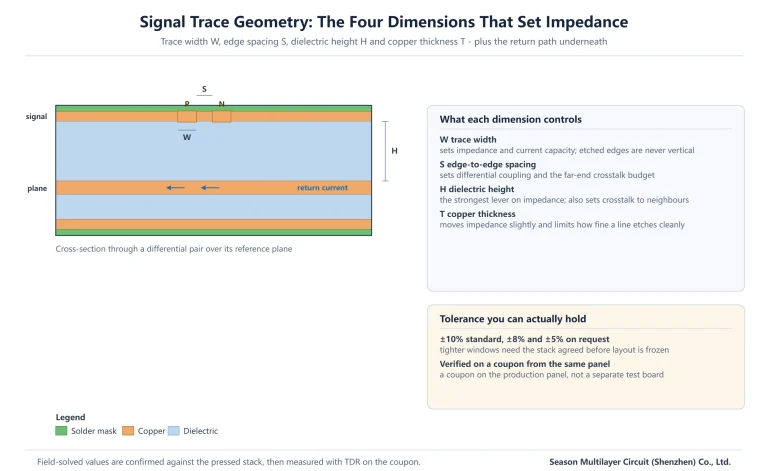
This is the decision that changed the build. The customer’s drawing asked for 1 oz on every layer. The impedance table asked for controlled single-ended and differential pairs on the inner layers. With 1 oz inner copper, the trace width needed for the target came out narrow enough that the etched edge tolerance became the dominant error term: thick copper etches with more undercut, the finished cross-section is more trapezoidal than the model assumes, and the spread across a panel and between panels grows.
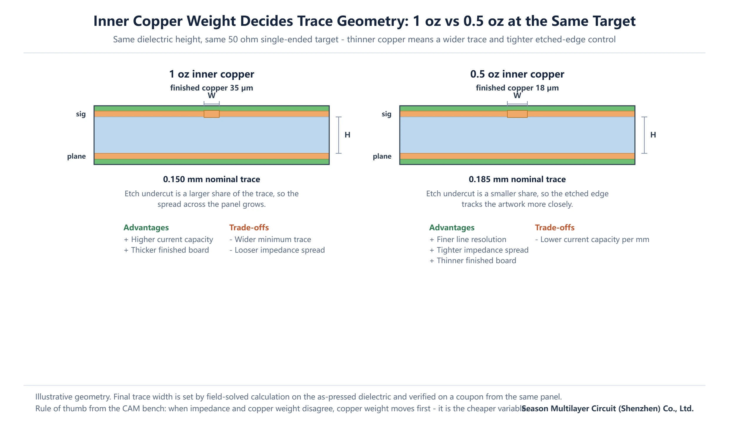
Moving the inner layers to 0.5 oz changed the geometry in a useful direction. For the same dielectric height and the same target, a thinner conductor needs a slightly wider trace, and the etched edge is closer to vertical. Wider is easier to hold, vertical is closer to the model, and the measured impedance lands nearer the calculation. The trade-off is real and has to be accepted deliberately: thinner inner copper carries less current and has higher DC resistance, and the board ends up marginally thinner.
| Decision axis | Inner 1 oz as drawn | Inner 0.5 oz as released |
|---|---|---|
| Finished inner copper | 35 µm | 18 µm |
| Trace width for the same target | Narrower | Slightly wider |
| Etched edge control | More undercut, more trapezoidal | Closer to vertical, closer to model |
| Achievable line and space | Wider limit | Finer limit |
| Current capacity per trace | Higher | Lower |
| Board thickness contribution | Thicker | Thinner |
The rule of thumb from the CAM bench is simple: when the impedance target and the copper weight disagree, move the copper weight first. It is the cheaper variable, it usually needs no layout change beyond a width tweak, and it does not alter the part placement or the board outline. Changing the dielectric height comes next, and changing the layer count is the expensive last resort.
None of this is applied silently. Every deviation is a proposal with a stated reason, and it goes back to the designer for approval before release – which is exactly what happened here. For the measurement side of the same story, including how the coupon is built and read, see our article on impedance measurement with TDR and coupons.
Retuning Trace Width and Spacing Against the Pressed Stack
Once the copper weights are settled, the widths are recalculated against the pressed dielectric rather than the nominal one. Prepreg does not stay at its catalogue thickness: resin flows during the press, and it flows differently next to a solid plane than next to a layer with sparse copper. A dielectric that measures thinner after pressing pushes impedance down, so the trace has to be narrowed to compensate, or the dielectric stack has to be adjusted.
The same review sets the etch compensation. Artwork is deliberately drawn wider or narrower than the finished target so that the etch process lands on the number, and that allowance is a function of copper weight – which is why the copper decision and the width decision have to be made together rather than in separate emails.
One consequence for designers: a tighter tolerance is only available if the stack is frozen before layout is finished. A ±10% window is the standard offer; ±8% and ±5% are available when the layer build-up, the copper weights and the coupon design are agreed in advance. Asking for a tight window after the artwork is complete usually means re-spinning the board rather than tuning the process.
Laminate Choice: What the Material Has to Survive
This build used a mid-to-high Tg FR-4 system rated at Tg 180, chosen for two reasons: the assembly is lead-free, and the panel sees more than one lamination cycle. Every extra press is another thermal excursion for the material, so decomposition temperature and the margin above the assembly peak matter more here than on a single-press board. Where a halogen-free specification is required, the equivalent grade sits at Tg 150 or above and is selected at the same review so the dielectric constants are consistent with the impedance model.
| Material property | Why it is checked on a multi-press build | Typical target |
|---|---|---|
| Glass transition (Tg) | Margin over the lead-free assembly peak temperature | Tg 150 to 180 by grade |
| Decomposition (Td) | Resistance to repeated lamination cycles | Confirmed per material datasheet |
| Flammability | End-product safety approval | UL 94 V-0 |
| Dk and Df | Sets trace width and insertion loss at the target frequency | Matched to the impedance model |
| CAF resistance | Long-term insulation resistance between plated holes | Required on fine-pitch designs |
Material selection is also where the compliance paperwork starts: RoHS and REACH declarations, UL recognition under UL 796 for the printed board, and the acceptance class under IPC-6012 that the board will be inspected against. Our laminate and materials guide lists the grades we hold and what each one is good for, and UL publishes its component recognition programmes for buyers who want to check the file themselves.
Laser Microvias, Buried Vias and the Through Holes That Remain
Microvia size is set by the laser process and the aspect ratio it can plate. On this class of build the standard laser microvia is 0.10 mm, with 0.076 mm available after review, and the plated aspect ratio is held at roughly 1:1 so the plating is reliable at the bottom of the hole. Stacked microvias are used here because the BGA pitch leaves no room to stagger them; where pitch allows, staggering reduces the stress concentration at the via stack.
Buried mechanical vias inside the core sub-board are drilled before build-up, at 0.20 mm minimum on this build, and they carry the connections that never reach the surface. Through holes are kept deliberately few: they are the cheapest hole per drill hit, but each one removes usable area on every layer it crosses, which is expensive on a board this dense. Where a through hole is unavoidable under a high-speed path and leaves a long stub, backdrilling removes it and is reviewed per board rather than assumed.
At fine BGA pitches the capture pad ends up inside the component pad, which pushes the design toward via-in-pad with a filled and capped hole. That is a process decision with cost and yield consequences, so it belongs in the same conversation as the copper weights, not in a footnote on the drawing.
First-Article Confirmation and In-Process Inspection
On a build with three press cycles, inspection cannot wait for the end. Each critical process step gets a first-article check before the rest of the lot is committed: drill programme and hole size after drilling, plating thickness after metallisation, imaging and development before etch, and registration measurement between layers after each press. The point is to catch a drift when it affects one panel instead of a batch.
- Automated optical inspection after each imaging step, so a pattern defect is found before it is buried under the next lamination cycle
- Registration measured between inner layers, since misregistration on a 16-layer board is what kills annular rings
- Electrical test – flying probe for prototypes, a fixture for volume – against the netlist from the released data
- Impedance measured with TDR on a coupon produced on the same panel, not on a separate test board
- Dimensional and visual acceptance against IPC-6012 Class 2, or Class 3 where the application is specified
- Final audit of surface finish thickness, solder mask coverage and legend legibility before shipment
The standard that governs acceptance here is IPC-6012, with IPC-A-600 as the visual reference for what a defect looks like. Both are maintained by the Global Electronics Association standards programme. If you want the detail of how a bare board is inspected end to end, our PCB manufacturing services page describes the flow step by step.
Cost and Lead Time: Where the Multipliers Come From
Cost on an HDI board is driven by cycle count, not by layer count alone. Each additional stage typically raises the cost by roughly 30% to 100%, because the panel repeats drilling, plating, imaging and registration for every build-up. That is why a 16-layer 2-stage HDI PCB costs materially more than a 16-layer through-hole board even though the copper and laminate inputs are similar.
The two changes described in this article are close to free by comparison. Changing an inner copper weight alters a material line item and an etch allowance; retuning trace width within the same design costs engineering time and nothing else. The expensive requests are the ones that add process: a tighter impedance window, via-in-pad with fill, a stage added late, or a panel shape that wastes laminate.
Lead time follows the same logic. As a reference point, an 8-10 layer 2-stage HDI prototype typically runs 17-18 working days from released data, and anything above that range – a 16-layer build included – is quoted after engineering review rather than guessed. What protects your schedule most is not urgency but completeness: a released stackup, an impedance table and a clean drill chart remove the review loops that actually consume the calendar.
Checklist Before You Release a 16-Layer 2-Stage HDI PCB
Most of the delay on boards like this comes from one missing item in the data package. The list below is what the review needs in order to return a buildable proposal instead of a list of questions. Where a decision is genuinely open, send it as a question rather than leaving it blank – a stated unknown is cheaper than a silent assumption.
| Item to send | What it decides | Typical content |
|---|---|---|
| Layer stackup with per-layer copper | Impedance model, etch allowance, total thickness | Layer order, copper weight, dielectric type and height |
| Impedance table | Trace width, tolerance class, coupon design | Target value, tolerance, layer, reference plane, nets |
| BGA pitch and breakout plan | Microvia size, stacked or staggered, via-in-pad need | Finest pitch, pad size, dogbone or via-in-pad |
| Material and Tg requirement | Laminate grade, halogen-free option, press profile | Tg, Dk/Df if controlled, halogen-free yes or no |
| Surface finish | Solderability, shelf life, wire bonding if any | ENIG, HASL, OSP or other, with thickness |
| Acceptance class and test | Inspection criteria and test coverage | IPC Class 2 or 3, electrical test, impedance report |
| Panel size and quantity | Utilisation, lead time, unit cost | Board dimensions, array layout, prototype or volume |
If you are still at the stackup stage, the PCB stackup design rules article covers how to assign planes and signal layers before the numbers are fixed, and the 14-layer 2-stage HDI prototype page shows a comparable build released at a slightly lower layer count.
Frequently Asked Questions
What is a 2-stage HDI PCB?
A 2-stage HDI build adds two build-up cycles to each face of a core sub-board, so a signal can step through two stacked laser microvias before reaching the core. On a 16-layer board the core carries the middle layers with buried mechanical vias, and the outer layers are added in two press and laser passes per side.
Why would a fabricator ask to change inner copper from 1 oz to 0.5 oz?
Thinner inner copper needs a slightly wider trace for the same impedance target, and it etches with less undercut, so the finished geometry is closer to the model and the measured impedance spread is tighter. The trade-off is lower current capacity and higher DC resistance on those layers.
Can a 16-layer 2-stage HDI PCB be built at 1.6 mm?
It can, but thinner total thickness means thinner dielectrics, which pushes traces narrower for the same impedance target and tightens the tolerance you can hold. This build was released at 2.0 mm with a ±0.20 mm window. Thinner targets are reviewed against the impedance table before they are accepted.
What impedance tolerance should I specify?
±10% is the standard window and covers most designs. ±8% and ±5% are available when the stackup, copper weights and coupon design are agreed before layout is frozen. Tighter windows increase engineering time and can reduce yield, so specify them where the interface needs them rather than board-wide.
How small can laser microvias be on this class of board?
The standard laser microvia is 0.10 mm, with 0.076 mm available after review, held at roughly a 1:1 plated aspect ratio so the plating is reliable at the bottom of the hole. Buried mechanical vias inside the core are typically 0.20 mm minimum on this build.
Do I need via-in-pad on a 16-layer HDI design?
Only when the BGA pitch leaves no room for a dogbone breakout. Via-in-pad requires the hole to be filled and capped flat so the solder joint is not starved, which adds process steps, so it is decided from the pitch and pad size rather than applied as a default.
How long does a 16-layer 2-stage HDI prototype take?
As a reference point, an 8-10 layer 2-stage HDI prototype typically runs 17-18 working days from released data. A 16-layer build carries more press cycles and inspection steps, so it is quoted after engineering review. Complete data – stackup, impedance table and drill chart – removes most of the review loops.
Have Your Stackup Reviewed Before the Numbers Are Fixed
Send the Gerber data together with your intended stackup, copper weights and impedance table, and the CAM review will come back with what is buildable as drawn and what needs to move. Deviations are returned as proposals with the reason attached, and nothing is released without your approval.
Our engineering team works from 2 to 30 layers, with laser microvias from 0.10 mm, minimum trace and space of 2/2 mil, and impedance control at ±10%, ±8% or ±5% depending on the stack agreed at review.