Book Appointment Now

A P3.91 LED module PCB is decided by four things: pad geometry inside the 3.91 mm cell, placement tolerance, copper budget for LED current and pad finish.
P3.91 LED Module PCB: Pad Geometry, Current and Finish
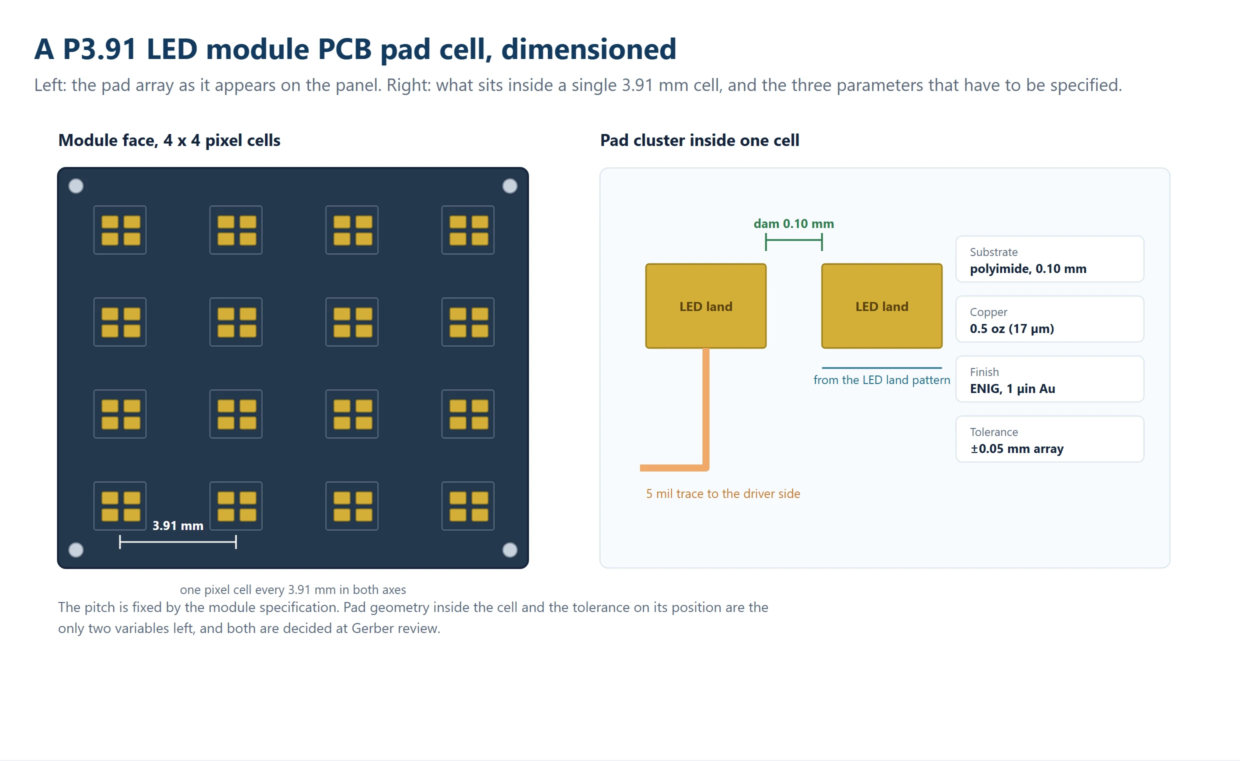
A P3.91 LED module PCB looks like the simplest board in a display. It is a rectangular array of pads on a thin substrate, and that apparent simplicity is exactly why first builds come back with brightness steps between pixels or a dark seam at the module joint. The pixel pitch fixes the pad array before anyone opens a CAD tool: 3.91 mm between LED centres leaves very little room for the pad, the solder mask dam beside it, and the routing that has to reach every pixel without stealing solderable area. This guide covers what actually decides yield on a P3.91 LED module PCB: pad geometry and placement tolerance inside the 3.91 mm cell, the copper budget that carries LED drive current, flatness and the thermal path, surface finish at fine pitch, laminate and thickness options, and the inspection evidence worth asking for. The parameters below are the values we build and quote against at Gerber review, not catalogue ranges.
Table of Contents
- What P3.91 Means on an LED Display Pad Board
- P3.91 LED Module PCB: The Reference Build We Quote Against
- Pad Geometry and Placement Tolerance Inside the Cell
- The Copper Budget Behind LED Drive Current
- Thermal Path and Flatness: Where Dark Lines Come From
- Surface Finish: ENIG Against HASL at Fine Pitch
- Laminate and Thickness Options for Pad Boards
- Inspection and Test Coverage to Ask For
- Ordering Checklist Before You Release Gerber Data
- What Moves the Cost of a P3.91 LED Module PCB
- FAQ
- Have the Pad Array Reviewed Before Tooling
What P3.91 Means on an LED Display Pad Board
P3.91 is the pixel pitch: 3.91 mm from the centre of one LED to the centre of the next, in both axes. On a 250 mm wide module that fixes a 64 pixel row, which in turn fixes how many pads exist, how much solderable area is available per pixel, and how much routing channel is left between them. Every later decision in the build follows from that one number.
The term pad board means the substrate that carries the LED pad array and the driver side interconnect. In practice it is a thin two layer panel, polyimide or FR-4, 125 mm to 250 mm square, with 5/5 mil routing and a solderable finish on the pads. It is not the driver IC board and it is not the receiving card; those are separate assemblies in the cabinet.
Because the pitch is locked by the module specification, the variables you still control are the pad geometry inside each 3.91 mm cell and the placement tolerance you can hold across the panel. Those two decide most of the yield difference between one fabricator and another, and both are cheap to specify at Gerber stage and expensive to correct after the first lot of LEDs is placed.
P3.91 LED Module PCB: The Reference Build We Quote Against
The table below is a working specification for a thin pad board, the kind of build that ships with an outdoor or indoor LED module today. Treat the panel size and mask as customer decisions and everything else as the process window that has to be met to hold pad position.
| Parameter | Reference value |
|---|---|
| Layer count | 2 layers |
| Base material | Polyimide (PI), flexible class substrate |
| Finished thickness | 0.10 mm |
| Panel size | 125 × 125 mm, or matched to the module frame |
| Copper weight | 0.5 oz (17 µm) finished |
| Minimum line and space | 5/5 mil |
| Minimum drilled hole | 0.20 mm |
| Pad placement tolerance | ±0.05 mm at fine pitch |
| Surface finish | ENIG, 1 µin gold over 3–5 µm nickel |
| Solder mask | Customer-specified |
| Electrical test | 100 percent flying probe |
Two items in that table change how the board is handled rather than how it is designed. At 0.10 mm the panel is thin enough to need carrier support through paste printing and reflow, so plan the fixture before you plan the run. And a 0.5 oz finished copper weight means the 5/5 mil traces are working close to the limit of what the thin substrate will hold after plating, which is why the copper budget in a later section matters more than it looks.
Pad Geometry and Placement Tolerance Inside the Cell
On a 3.91 mm pitch the pad pitch is generous compared with P1.5 work, so the classic failure is not pad to pad bridging. It is positional drift: pad centres wandering relative to the LED body, which shows up as tombstoning on small parts, tilted components after reflow, and brightness steps that only appear when a full module is switched on at a low grey level.
| Dimension | Coarse pitch, P3 and above | Fine pitch, P2 and below |
|---|---|---|
| Pad placement tolerance | ±0.10 mm | ±0.05 mm |
| Base material | Standard FR-4 | Low expansion Tg 170–180 grade |
| Flatness requirement | Standard bow limit | Module-joint class |
| Dominant finish | HASL | ENIG |
| Solder mask dam | 0.10 mm minimum | 0.08–0.10 mm, tightly inspected |
| Relative cost factor | 1.0 baseline | Roughly 1.5x the baseline |
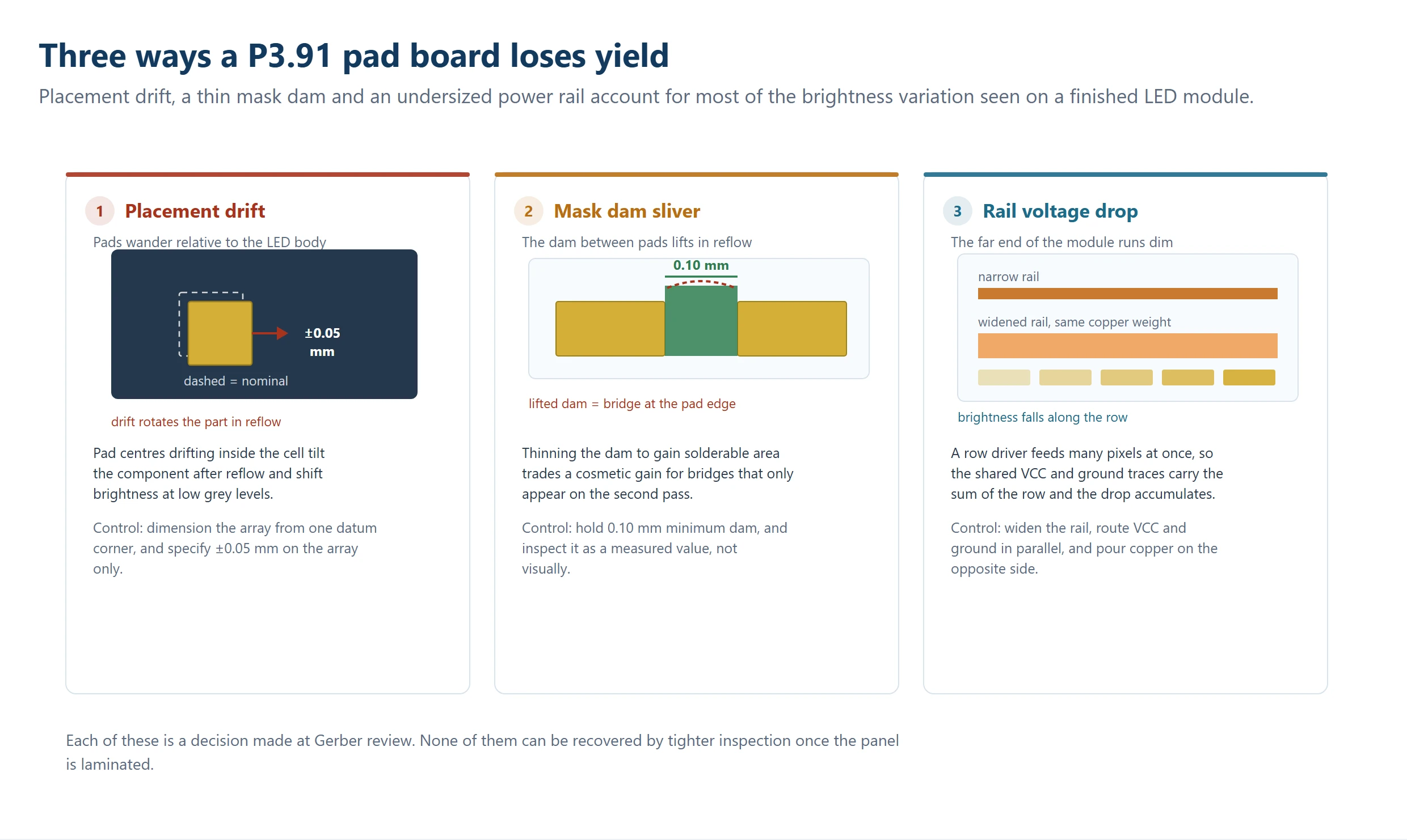
The mask dam is the detail that catches teams out. It is the strip of solder mask between two adjacent pads on the same net group, and it is usually specified at 0.10 mm minimum on this pitch. Push it thinner to gain solderable area and the dam lifts during reflow, the solder bridges, and the defect only appears after the second pass because the first pass looked clean.
Pad geometry itself should follow the LED land pattern rather than a house rule. Ask the LED supplier for the recommended land, keep the pad 0.05 mm to 0.10 mm larger per side than the terminal if a custom land is needed, and dimension the array from a single datum at one corner of the module. Arrays dimensioned from the panel centre accumulate half the tolerance twice and drift at the edges.
The Copper Budget Behind LED Drive Current
Current per pixel on a P3.91 module is modest, tens of milliamps in most scan schemes. The problem is not one pixel, it is the shared rail: a row driver feeds many pixels at once, so the VCC and ground traces carry the sum of the row, and the voltage drop accumulates along the trace until the far end of the module is visibly dimmer than the near end at full white.
At 0.5 oz finished copper the sheet resistance is roughly 1 mΩ per square. Multiply by the number of squares in the run and you have the drop for a given current. The cheapest fix is geometric: widen the rail, route VCC and ground as parallel traces, and add a copper pour on the non-component side so the return path has somewhere to go. Copper weight design rules cover when heavier copper is the right answer.
The trap is reaching for heavier copper to fix a drop problem on a thin substrate. Going from 0.5 oz to 1 oz on a 0.10 mm polyimide panel changes etch behaviour at 5/5 mil, tightens the process window and pushes cost up, often for less gain than simply widening the trace by 0.1 mm. On a pad board, width is cheaper than weight.
Thermal Path and Flatness: Where Dark Lines Come From
LED output falls as junction temperature rises, so the pad board is the first thermal layer in the stack. Copper area under and around each pad, the presence or absence of thermal vias, and the flatness of the panel together decide whether a finished module shows a hot band along the driver edge after an hour of operation. On thin substrate the copper is also the only heat spreader available.
Flatness matters at the joint. Adjacent modules on a screen are butted to within a fraction of a millimetre, so a 0.10 mm bow across a 250 mm module reads as a visible dark line between cabinets. Balanced copper distribution on both sides of a two layer board is the practical control: keep the copper area on the component side and the opposite side within about 20 percent of each other before lamination.
This is where substrate choice stops being a cost argument. Polyimide tolerates thinness and heat, FR-4 tolerates flatness above 0.8 mm and costs less. A 0.10 mm polyimide panel with unbalanced copper will bow more than a 1.0 mm FR-4 panel with the same artwork, and no amount of stencil tuning fixes a bowed module.
Surface Finish: ENIG Against HASL at Fine Pitch
HASL leaves a meniscus that varies in height across the pad, and on a 3.91 mm pitch that variation is still tolerable if the pad is generous and the assembly house tunes the stencil. ENIG gives a flat, coplanar pad with predictable wetting, which is why it becomes the default once the pitch drops below P2 or the LED land pattern gets tight.
Gold thickness for a solderable finish is often quoted at 1 µin over 3–5 µm of nickel, and that is enough. Thicker gold does nothing for soldering and adds cost; it exists for wire bonding and for edge contacts, not for SMT pads. The finish problem worth worrying about is not thickness but nickel bath control, which produces the black pad failure mode described in the ENIG solderability guide.
For outdoor modules, mask and finish selection is driven by ultraviolet exposure and thermal cycling rather than appearance. Specify the mask class and the finish, and leave the colour as a customer decision. A dark mask on an outdoor module absorbs more heat, so if the cabinet has no active cooling, that is a thermal decision rather than a cosmetic one.
Laminate and Thickness Options for Pad Boards
Four builds cover most of what comes through quotation on this pitch. The right one is decided by module size, mounting method and whether the board is expected to flex during assembly or service.
| Option | Thickness | Where it fits | Watch out for |
|---|---|---|---|
| Polyimide, 2 layer | 0.10 mm | Thin indoor modules, curved and irregular frames | Needs carrier support through SMT; copper balance critical |
| FR-4, Tg 150 mid-Tg | 0.80 mm | Standard indoor fixed modules | Bow rises on large panels if copper is unbalanced |
| FR-4, Tg 170 grade | 1.00 mm | Outdoor cabinets with wide temperature swing | Slightly higher lamination cost than Tg 150 |
| FR-4, Tg 180 grade | 1.60–2.00 mm | Large modules and mechanical load bearing frames | Heaviest option; check cabinet weight budget |
When the choice is open, work from the temperature swing and the mounting method first, then from cost. The laminate selection guide covers the electrical side of the same decision, including halogen-free grades such as S1150G for projects with a materials restriction.
Inspection and Test Coverage to Ask For
On a pad board the defect that hurts is the one you cannot see: a pad that is 0.05 mm off, a mask dam that is thinner than the artwork, or a plated hole with marginal copper in the barrel. Optical inspection catches the first two, flying probe catches opens and shorts, and neither catches plating thickness, which is why first article cross sections matter more here than on a dense digital board.
Ask for three things and the quality conversation gets concrete: a coordinate measurement report on pad positions from the first article, a cross section of hole copper and surface copper from the same article, and a solderability check per lot if the modules will be assembled on site. References to IPC acceptance standards belong in the purchase order, with the class named explicitly rather than left to interpretation.
Impedance control is normally not a requirement on a LED pad board, since the traces carry DC and low frequency switching rather than serial data. If your design does include a long differential pair for a receiver card interface, say so at quotation, because controlled impedance changes the stackup and the coupon requirement.
Ordering Checklist Before You Release Gerber Data
Most pad board rework traces back to information that was never sent, not to a process failure. The list below is the minimum package we need to build without assumptions.
- Gerber data with drill file, and the pad array dimensioned from one datum corner
- Pixel pitch and array count per panel, plus the module outline and any frame relief
- Copper weight and minimum trace width, with the current each rail has to carry
- Surface finish and gold thickness, split by area if the board has both pads and edge contacts
- Solder mask specification, and whether the mask may be thinned between pads
- Panel size, bow limit and the handling method for thin substrate
- Test requirement and the report package you expect with the shipment
Send the package with the module drawing attached, not just the board file. The module drawing is what tells a fabricator that a 0.05 mm pad shift is a brightness problem rather than a cosmetic one, and that context changes how the panel is tooled. The P3.91 LED module PCB product page lists the build envelope we hold, and the manufacturing capability page covers the layer count and via range around it.
What Moves the Cost of a P3.91 LED Module PCB
On this product the bill of process is short, so cost is dominated by three things: how well the array fits the panel, which finish you specify, and how tight the tolerance class is. Layer count rarely moves because two layers is already the answer.
| Cost driver | Effect | How to control it |
|---|---|---|
| Panel utilisation | Largest single factor | Match panel size to the array; 125 mm and 250 mm frames tile differently |
| Surface finish | ENIG roughly 1.1–1.3x HASL | Use HASL above P3 where the land pattern allows |
| Minimum line and space | 5/5 mil is the cost step | Do not ask for 4/4 mil unless the LED land demands it |
| Tolerance class | ±0.05 mm adds inspection and scrap | Specify fine tolerance only on the pad array, not on the whole board |
| Substrate | Polyimide above FR-4 | Use FR-4 where the module does not need thinness |
| Test and report package | Adds steps, not material | First article only; skip per-lot CMM unless the customer requires it |
The multipliers above are relative, not absolute prices, and the real number always comes back from a Gerber review where panel utilisation is calculated against the actual array. If a quote is well outside the band these factors predict, the usual cause is a panel that tiles badly, for example a 250 mm module array dropped onto a 125 mm panel with 30 percent waste.
Frequently Asked Questions
What is a P3.91 LED module PCB?
It is the thin substrate that carries the LED pad array and driver side interconnect inside a display module with a 3.91 mm pixel pitch. Typical builds are two layer panels in 0.10 mm polyimide or 0.8–2.0 mm FR-4, with 5/5 mil routing, 0.5 oz to 1 oz copper and an ENIG or HASL pad finish.
What does the 3.91 in P3.91 actually mean?
It is the distance in millimetres between the centres of two adjacent LEDs, measured in both axes. A 3.91 mm pitch is a mid-range indoor and outdoor product: coarse enough for HASL and standard FR-4 in many cases, fine enough that pad placement tolerance and mask dam width start to matter.
Which surface finish should I specify for a P3.91 pad board?
ENIG with 1 µin gold over 3–5 µm nickel is the safe default because the pad stays flat and wets predictably. HASL works above P3 when the land pattern is generous and the assembly house controls the stencil. If the module goes outdoors, choose the finish together with the mask class rather than on appearance.
Can a P3.91 LED module PCB be built on FR-4 instead of polyimide?
Yes, and most fixed indoor modules are. Polyimide is chosen for thinness, curved frames and heat, at the cost of flatness control and the need for carrier support during assembly. FR-4 from 0.8 mm upward is cheaper and flatter, but heavier, which matters if the cabinet has a weight budget.
What placement tolerance can be held on LED pads?
±0.05 mm is achievable on the pad array of a fine pitch board with a dedicated tooling hole scheme, and ±0.10 mm is normal for coarse pitch. The tolerance should be specified on the array only, not on the whole panel, because applying a fine tolerance board wide adds inspection steps and scrap without improving the display.
How is the cost of a P3.91 pad board calculated?
Panel utilisation dominates, then surface finish, minimum line and space, tolerance class and substrate. Layer count rarely changes because two layers is already sufficient. Quotes are built from the actual array tiling rather than a price per square metre, so a panel that tiles badly can cost noticeably more than the same area tiled well.
Does a P3.91 LED module PCB need impedance control?
Normally no. The traces carry DC and low frequency switching current rather than serial data, so controlled impedance adds cost without benefit. The exception is a board that also carries a long differential pair for a receiver card interface; if that is in your design, declare it at quotation because it changes the stackup and the test coupon.
Have the Pad Array Reviewed Before Tooling
Send the Gerber data together with the module drawing and the pitch, and we will come back with pad geometry, panel tiling and the finish that fits the cabinet. Thin substrate builds are quoted after a review of the array, not from a catalogue number.
If the module is still in layout, the PCB manufacturing services overview explains what a DFM pass covers before the first panel is cut.