Book Appointment Now

4-layer PCB cost explained without price lists: the five variables that move a quote, relative layer-count multipliers, and prototype vs production economics.
4-Layer PCB Cost: What Drives the Price and How to Quote It Right
Collect three quotes for the same four-layer design and you will often get three different numbers. The spread is not random: 4-layer PCB cost is driven by a small set of variables — laminate grade, surface finish, copper weight, order quantity and lead time — interacting with how a factory loads its lamination and drilling queues. This guide breaks the cost apart piece by piece so you can tell a fair quote from an inflated one.
You will get a relative cost ladder from 2-layer to 8-layer builds, the five variables that move a 4-layer quote the most, how prototype pricing differs from production pricing, and a submission checklist that gets you a number you can act on. Throughout, figures are expressed as relative multipliers rather than absolute prices, because board pricing moves with copper, gold and order profile.
Table of Contents
- What 4-Layer PCB Cost Actually Pays For
- How 4-Layer PCB Cost Scales With Layer Count
- The Five Variables That Move a 4-Layer Quote
- Prototype vs Production: How Volume Changes Unit Price
- 4-Layer vs 2-Layer: What the Extra Money Buys
- Typical 4-Layer Stackups and Their Cost Impact
- Where 4-Layer PCB Cost Can Be Cut Safely
- Spec Mistakes That Inflate a 4-Layer Quote
- From Gerber to Firm Quote: What to Submit
- FAQ
- Get Your 4-Layer Stackup Reviewed Before You Order
What 4-Layer PCB Cost Actually Pays For
Every 4-layer quote has two components that behave very differently. The first is the material component: base laminate, prepreg, copper foil, plating chemistry and surface-finish metals, all of which scale with board area and copper weight. The second is the engineering component: photo tools for each layer, drill files, electrical-test fixtures, stackup review and process setup. The engineering component is largely fixed — it costs the fabricator nearly the same whether you order five boards or five hundred.
This is why small prototype invoices are dominated by engineering charges rather than by raw material. A 50 mm × 50 mm four-layer prototype uses very little laminate, yet it still consumes one full set of tooling, one drill program and one test fixture. When buyers compare quotes from different factories at prototype quantity, they are mostly comparing how each factory amortizes and discounts that fixed engineering package.
The practical consequence: at prototype scale, negotiating laminate brands or copper weights moves the needle far less than consolidating designs onto fewer orders or reusing an existing panel. At production scale the balance flips, and material grade, panel utilization and yield become the dominant cost levers.
How 4-Layer PCB Cost Scales With Layer Count
Layer count is the single largest cost lever, because every additional lamination cycle adds inner-layer imaging, oxide treatment, press time and lamination-alignment control. Using a conventional four-layer FR-4 build as the baseline of 1.0, the relative ladder for nearby layer counts looks like this:
| Build | Relative cost index (4-layer = 1.0) | What the increment buys |
|---|---|---|
| 2-layer (double-sided) | ≈ 0.4× | No internal layers; return paths depend on scattered ground traces |
| 4-layer | 1.0× (baseline) | Complete internal ground and power planes, controlled-impedance ready |
| 6-layer | ≈ 1.5× | Two more signal layers or dedicated signal/return pairing for faster edges |
| 8-layer | ≈ 2.2× | Extra routing channels for dense BGA fanout and better EMI containment |
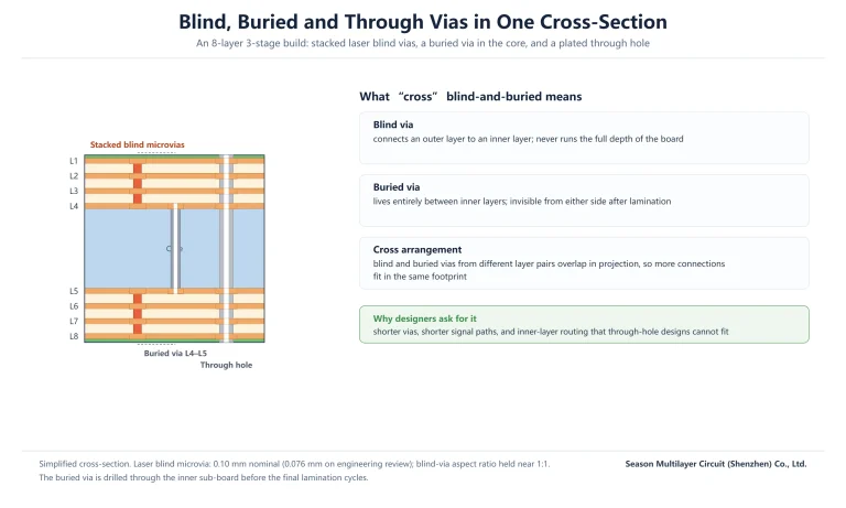
Two patterns are worth internalizing. First, each step up the ladder adds roughly fifty percent to a doubling of layer count, so jumping from 4 to 6 layers is proportionally cheaper per added layer than jumping from 2 to 4. Second, the ladder assumes conventional through-hole construction. Blind and buried vias, heavy copper and HDI stackups are priced as separate process premiums on top of the layer ladder, which is why two “8-layer” quotes can differ by a wide margin if one includes sequential lamination and the other does not.
The Five Variables That Move a 4-Layer Quote
Beyond layer count, five variables explain most of the spread in 4-layer PCB cost between quotes for an identical design. The table below uses the same relative framing — a conventional FR-4 build with HASL finish and standard copper as the baseline:
| Variable | Typical relative impact | Practical note |
|---|---|---|
| Laminate grade | Mid-Tg or Tg 170 grades ≈ +10–30%; low-loss and PTFE-based RF materials can reach 2–5× or more | Match glass transition and dissipation factor to the assembly profile and signal speeds; see the laminate selection guide |
| Surface finish | ENIG prices above a HASL baseline, scaled with pad density | Choose by assembly process — flatness for fine-pitch BGA, solderability for wave soldering |
| Copper weight | Moving outer layers to 2 oz copper adds roughly 20–40% | Heavier copper also loosens minimum trace capability and affects etch control |
| Order quantity | Volume unit price can fall to roughly 1/3–1/5 of the prototype price | Fixed engineering fees amortize across the production panel count |
| Lead time | Expedited options are priced case by case | Confirmed at engineering review — never assume a default expedite premium |
When comparing quotes, align these five first. A quote on a Tg 170 laminate with ENIG is not comparable to one on standard Tg 130 material with HASL, and treating them as equivalents is the fastest way to buy a problem. For a structured walk through dielectric options, our PCB materials and laminates guide covers the selection logic in depth; it is also worth confirming the chosen grade carries the appropriate UL recognition for your end market before locking the bill of materials.
Prototype vs Production: How Volume Changes Unit Price
Buyers searching for what a single board costs are really asking two different questions. The material part of a prototype is small — a 100 mm × 100 mm four-layer panel consumes laminate worth only a modest fraction of the invoice. The engineering part is the heavy hitter: films, drill data, test fixtures and setup exist whether the order is one panel or one hundred.
As volume rises, that fixed engineering package spreads across more panels, which is why volume unit pricing can reach roughly one third to one fifth of the prototype unit price for the same design. Production orders also add their own cost layer — 100% electrical test, automated optical inspection and X-ray checks on inner layers — but these scale efficiently and are already reflected in volume pricing.
One underrated lever at both scales is panel utilization. A board outline that nests efficiently into a standard production panel can lower the effective per-board material cost without changing anything electrical. Before finalizing an outline, it is worth asking your fabricator which panel formats they run; a 5 mm outline adjustment occasionally buys a meaningful price step.
4-Layer vs 2-Layer: What the Extra Money Buys
At roughly 2.5× the relative price of a double-sided board, a four-layer build needs to justify itself structurally. The justification is the pair of internal planes. With a complete ground plane adjacent to every signal layer, return currents have an uninterrupted path, loop inductance drops, and crosstalk between routing channels falls sharply. The same construction is what makes impedance control routine rather than an exercise in trace archaeology.
For products with clocked digital logic, wireless modules or any controlled-impedance nets, this structural upgrade often costs less overall than the alternative: a 2-layer design that passes the bench but fails radiated-emissions testing, then consumes weeks of ferrite-and-respin iteration. The plane pair is, in effect, pre-paid EMC margin.
The board type also carries across a wide product range — the same four-layer construction serves as a networking router PCB, an automotive electronics PCB and a SATA SSD storage PCB. What changes between those applications is not the layer count but the reliability requirements, material choices and test intensity — differences that show up in the five variables above rather than in the layer ladder itself.
Typical 4-Layer Stackups and Their Cost Impact
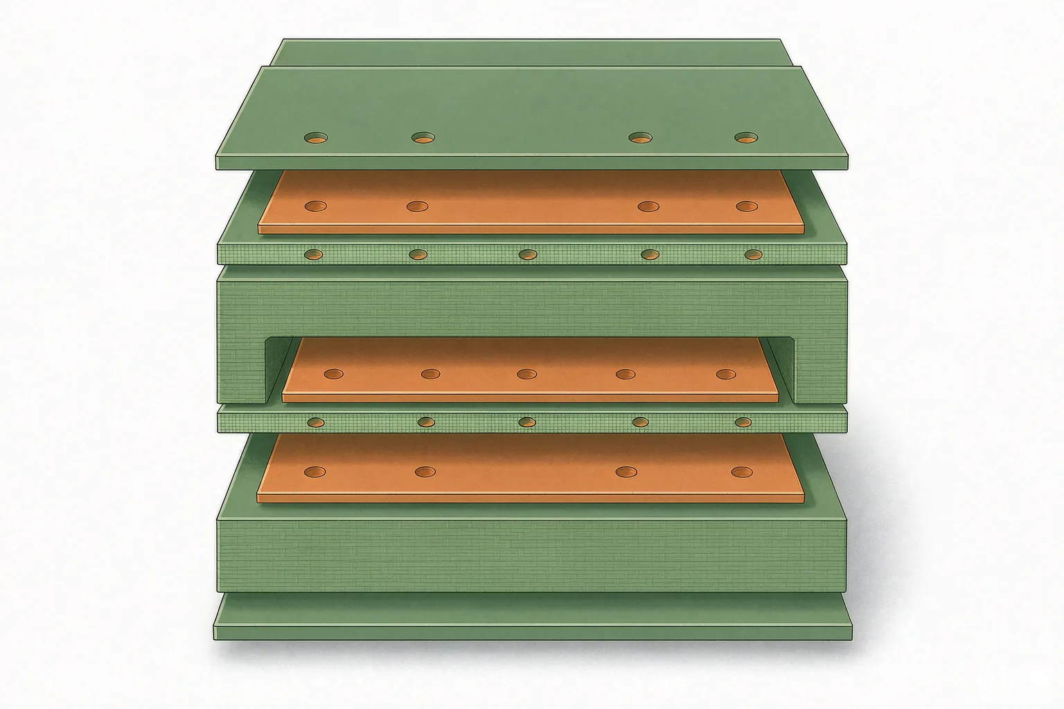
The most common four-layer construction for a 1.6 mm finished board assigns the two inner layers to ground and power, with signal routing on both outers. This symmetric arrangement matters commercially as well as electrically: a balanced stackup presses flat, while an asymmetric one invites warp that shows up as reflow or fixture problems downstream.
| Layer | Typical assignment | Cost-relevant role |
|---|---|---|
| L1 (outer) | Signal and components | Outer imaging, solder mask and surface finish are applied here |
| Prepreg | Bonding dielectric | Prepreg thickness and resin system set impedance; specialty fills add cost |
| L2 (inner) | Ground plane | Return path for L1 signals; a solid plane is inexpensive reliability |
| Core | Base laminate | Core grade and thickness drive the material share of the quote |
| L3 (inner) | Power plane | Low-impedance distribution that shrinks the external decoupling network |
| L4 (outer) | Signal and components | Mirrors L1; symmetry with L1–L2 limits post-lamination warp |
Impedance targets ride on this stackup. Single-ended 50 Ω and differential 90–100 Ω pairs are routine controls on four-layer builds. Tolerance expectations should be realistic: ±10% is the standard production tolerance, with ±8% and ±5% achievable per stackup review for designs that genuinely need it. Every tightening step constricts the press and etch windows, and the quote reflects that — so specify tight tolerances only on nets whose timing budget demands them.
Where 4-Layer PCB Cost Can Be Cut Safely
Meaningful 4-layer PCB cost reduction rarely comes from haggling; it comes from removing specification that the application does not use. The reliable levers:
- Choose the laminate by assembly profile and signal speed, not by brand reflex — many designs run perfectly on mid-Tg FR-4 while paying nothing for RF-grade material
- Keep impedance tolerance at ±10% unless a specific interface requires tighter control
- Select surface finish by process: HASL where solderability is the only requirement, ENIG for fine-pitch flatness, OSP where the assembly flow suits it
- Keep the outline panel-friendly and avoid unnecessary edge castellations or odd shapes that waste production panels
- Consolidate prototype variants into one order so engineering charges are paid once, not per revision
Each of these trims cost without touching the reliability structure of the board. The inverse approach — cutting corner radius on press capacity, skipping e-test, or downgrading copper thickness under a power plane — tends to reappear later as yield loss or field returns, which is the most expensive form of savings.
Spec Mistakes That Inflate a 4-Layer Quote
Fabricators price risk. When a drawing is ambiguous or over-specified, the quoted number carries a cushion for every interpretation the factory might have to absorb. The most common self-inflicted cost bumps on four-layer orders:
- Blanket tight tolerances applied to every feature instead of the few that matter
- Requesting an inspection class the application does not need — IPC Class 3 requirements cost more to produce than Class 2, and many consumer and industrial products gain nothing from them
- Undefined stackup: no layer assignment, no impedance targets, forcing the factory to quote conservatively
- Mixed signals in the data set — Gerber files that disagree with the drill file or the fabrication drawing
- Last-minute surface-finish or material changes after the quote, restarting engineering review
The last item deserves emphasis. Every post-quote revision re-opens tooling and stackup review, and the requote almost always lands above the original. Freezing the specification before requesting pricing is the cheapest schedule protection available.
From Gerber to Firm Quote: What to Submit
A complete submission collapses the quoting cycle from days to hours. Export Gerber data in RS-274-X format with embedded apertures, and pair it with a short specification note covering the five variables above. The minimum set:
- Board outline and finished thickness (1.6 mm is the common default for four-layer builds)
- Layer stackup with copper weights and which layers carry planes
- Impedance targets and which nets they apply to, if any
- Laminate grade, surface finish and solder-mask color
- Quantity split between prototype and follow-on production, plus the required delivery window
With that package, engineering review can confirm manufacturability and return an itemized quote — typically within 24 hours, including a fixed shipping schedule. If the design is still at schematic stage, board outline and layer count alone are enough to get a reference range to budget against. You can start from the online quote page or read how the PCB manufacturing services team handles design reviews end to end.
Frequently Asked Questions
How much more does a 4-layer PCB cost than a 2-layer board?
Using a conventional FR-4 four-layer build as the baseline, a double-sided board sits at roughly 0.4× of the same area — meaning the 4-layer runs about two and a half times the double-sided price. The difference buys the two internal planes: shorter return paths, better EMC behavior and routine impedance control. For designs with any speed or emissions sensitivity, that structure usually repays itself in avoided respins.
Why do 4-layer PCB quotes differ so much between suppliers?
Because quotes embed different assumptions. One factory may price a Tg 170 laminate with ENIG while another assumes standard FR-4 with HASL; one may include full impedance verification while another quotes it as an extra. Engineering-fee amortization policies also differ. Aligning the five variables — material, finish, copper weight, quantity and lead time — before comparing numbers removes most of the spread.
What is included in 4-layer PCB prototype pricing?
A prototype invoice is dominated by fixed engineering charges: photo tools for each of the four layers, drill programs, electrical-test fixtures and stackup review. The material itself is a minor share at small quantities. This is why the per-board prototype price is much higher than the volume unit price, and why consolidating several prototype designs into one order lowers the effective engineering cost per design.
Does impedance control add much to 4-layer PCB cost?
Impedance control on a four-layer board typically adds a relative reserve in the region of 10–25% to the quote, depending on tolerance and test requirements. Single-ended 50 Ω and differential 90–100 Ω are routine. Tolerance matters: ±10% is the standard production window, while ±8% and ±5% are achievable per stackup review and carry a premium, so apply tight tolerances only where timing budgets require them.
Which surface finish is most cost-effective for a 4-layer board?
HASL remains the cost baseline where solderability is the only requirement. ENIG costs more and is justified when flatness matters — fine-pitch BGA packages, castellated edges or backplane connectors. OSP sits between them and suits assembly flows that avoid multiple reflow cycles. The right answer follows the assembly process and component mix rather than a universal default.
Can a 4-layer board be upgraded to HDI later?
Yes. Four-layer HDI constructions with laser microvias are in regular production, combining the standard four-layer plane structure with 1-stage microvia interconnect. The upgrade changes the process premium — sequential lamination and laser drilling price separately from the layer ladder — so it is best decided at design time rather than retrofitted, though a stackup review can usually tell you quickly whether your current design tolerates the conversion.
How can I reduce my 4-layer PCB cost without hurting reliability?
Remove specification the application does not use: mid-Tg laminate instead of a premium grade where signal speeds allow, ±10% impedance tolerance instead of tighter windows, surface finish chosen by assembly process, panel-friendly outlines, and consolidated ordering so engineering charges amortize once. All of these leave the electrical and thermal structure intact. Cutting e-test, plane copper or press quality does not — those savings resurface as yield loss and field returns.
Get Your 4-Layer Stackup Reviewed Before You Order
The fastest way to pin down your 4-layer PCB cost is to submit the Gerber set together with the five-variable specification note. Engineering review will confirm manufacturability, flag over-specification, and return an itemized quote, typically within 24 hours with a fixed shipping schedule. For how per-area pricing behaves across layer counts, see our PCB cost per square meter breakdown; if your build adds laser microvias on a four-layer base, the 4-layer 1-stage HDI LED display PCB page shows that construction in production.