Book Appointment Now

What happens inside PCB inner layer fabrication — dry film, exposure, etching and AOI — and the line and spacing rules designers must respect.
PCB Inner Layer Fabrication: Dry Film, Etching and AOI
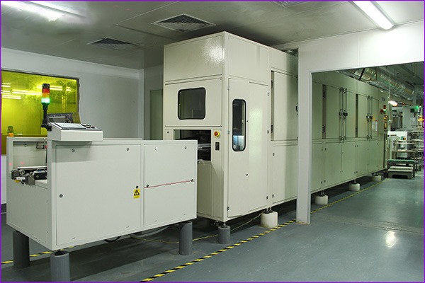
An open trace on an outer layer of a PCB can sometimes be patched with a wire. An open trace buried inside a laminated multilayer board usually means the panel is scrap. That asymmetry is why PCB inner layer fabrication is policed harder than almost any other step: once the layers are pressed together, nothing inside can be inspected, reworked or forgiven. Every open, short and spacing violation that survives this stage is sealed into the stackup permanently.
This guide walks the process in order — dry film lamination, exposure, develop, etch, strip and AOI — from the point of view of the engineers and buyers who specify these boards. Along the way it covers the choices that shape fine-line capability, the chemistry rules that decide line quality, and the design rules your layout must respect so the inner layers come off the line right the first time.
Table of Contents
- What PCB Inner Layer Fabrication Produces
- The PCB Inner Layer Fabrication Flow, Step by Step
- Dry Film Lamination: Temperature, Pressure and Speed
- Dry Film vs Liquid Photoresist on Inner Layers
- Exposure: Contact, Projection and Laser Direct Imaging
- Develop: Where Fine Lines Survive or Wash Away
- Inner Layer Etching: Chemistry and Etch Factor
- Strip and AOI: Catching an Open Before It Is Sealed Inside
- Design Rules for Inner Layers: Width, Spacing and Copper Balance
- Print-and-Etch vs Pattern Plating: Why Inner Layers Are Different
- FAQ
- Have Your Inner Layers Engineered Before They Are Sealed
What PCB Inner Layer Fabrication Produces
Inner layers are the circuit planes that will live inside the finished board: signal routing, power and ground planes, and the buried patterns that outer layers connect to through drilled and plated holes. They start as copper-clad cores — panels cut and staged as described in our PCB panel cutting guide — and they leave this stage as fully patterned, inspected copper images, ready for oxide treatment and lamination.
The transformation is subtractive: the core arrives fully clad in copper, and the process removes everything that is not circuit. A photosensitive resist defines where copper survives, etchant removes the rest, and the resist is stripped away. That simplicity is deceptive, because every step has a window — of temperature, energy, concentration or time — and yield lives inside those windows.
Buyers rarely see this stage, yet it determines more of the final board’s character than any other. Layer-to-layer registration, impedance geometry, plane reliability and the board’s long-term insulation resistance all trace back to decisions made here, on panels nobody will ever look at again after lamination. It is the discipline behind the multilayer PCB manufacturing capability a fabricator claims on its website.
The PCB Inner Layer Fabrication Flow, Step by Step
The sequence is consistent across the industry: clean, laminate resist, expose, develop, etch, strip, inspect. What separates a high-yield line from a struggling one is how tightly each step holds its window, and how quickly defects are caught. The table below summarizes what each step controls and what typically goes wrong when it drifts.
| Step | What is controlled | Typical failure if it drifts |
|---|---|---|
| Incoming clean | Contamination and oxidation on the copper foil | Resist adhesion voids that etch into opens |
| Dry film lamination | Roll temperature, pressure and speed | Bubbles, wrinkles and film lifting during develop |
| Exposure | Energy, vacuum and artwork or LDI registration | Thinned or widened traces from under- or over-exposure |
| Develop | Solution concentration, temperature, break-point | Residue in fine spaces that etches into shorts |
| Etch | Chemistry, concentration and spray pressure | Overetched thin or open traces; underetched spacing violations |
| Strip | Caustic concentration and temperature | Resist residue that degrades oxide adhesion |
| AOI | Alignment reference and defect thresholds | Opens or shorts sealed into the stackup at lamination |
Notice how the failure column compounds: a laminating flaw becomes an etching defect, which becomes a scrapped multilayer panel. This is why inner-layer lines run with process control discipline closer to a semiconductor fab than to a machine shop, and why reputable fabricators are willing to show buyers their AOI data for critical layers.
Dry Film Lamination: Temperature, Pressure and Speed
Dry film photoresist arrives as a roll: a polyester carrier, a photoactive acrylate layer, and a polyethylene separator. The laminator heats the film, presses it onto the copper under calibrated rolls, and leaves a uniform, bubble-free coating ready for exposure. If you want the materials science behind this layer, our PCB photoresist guide covers how the chemistry works in depth.
Three parameters govern the outcome. Temperature must be high enough to soften the film so it wets the copper, but not so high that it becomes fragile. Pressure must squeeze out air without thinning the film over raised features. Speed sets the residence time and, with the other two, decides whether the film conforms cleanly across the whole panel including edges and previous tooling features.
Get lamination wrong and the defects do not appear immediately. A microscopic bubble under the resist survives develop, becomes an unprotected copper island during etch, and turns into a conductive sliver or a spacing violation discovered only at AOI — or worse, not until a customer’s microsection. Lamination quality is invisible at the moment it matters, which is why the parameter windows are locked and audited rather than tuned by feel.
Dry Film vs Liquid Photoresist on Inner Layers
Some fabricators also run liquid photoresist on inner layers — a liquid, light-sensitive coating applied by screen or curtain. Each system has a place, and the choice is usually driven by the pattern being built rather than by cost alone:
| Property | Dry film (solid photoresist) | Liquid photoresist (wet film) |
|---|---|---|
| Application | Hot-roll laminated with uniform thickness | Screen- or curtain-coated, thickness varies with control quality |
| Fine-line uniformity | Strong, thickness is set by the film itself | Good, but depends heavily on coating discipline |
| Edge and surface coverage | Conforms over the full panel consistently | Can thin over edges without tight process control |
| Handling | No drying step, cleanroom-friendly | Requires drying time and stricter environment control |
| Typical use | Standard multilayer inner layers and fine lines | High-volume simpler patterns and special processes |
For fine-line inner layers — the 2/2 mil class and below that modern digital and industrial products demand — dry film’s thickness uniformity is the reason it dominates. A resist that varies in thickness etches unevenly, and uneven etch is the enemy of controlled impedance. When a fabricator quotes tight line-width tolerances, the answer behind that quote is usually a well-maintained dry film line.
Exposure: Contact, Projection and Laser Direct Imaging
Exposure transfers the artwork into the resist. In classic contact printing, an artwork film is pressed against the panel under vacuum and flood-exposed with UV. It is fast and sharp, but the film touches the panel, so it wears, attracts contamination and — critically — must be aligned to each layer with mechanical precision.
| Exposure method | How it works | Strengths | Watch-outs |
|---|---|---|---|
| Contact exposure | Artwork film pressed to the panel under vacuum, flood UV | High resolution, fast per panel | Film wear and dirt transfer; manual alignment limits |
| Projection exposure | Image optically projected onto the panel | No film contact, longer film life | Alignment optics add setup time and cost |
| Laser direct imaging (LDI) | Laser writes the pattern straight from data | No film at all; best registration; fine-line friendly | Lower throughput per machine; highest capital cost |
The registration angle deserves emphasis for multilayer buyers. Each inner layer is exposed independently, and the layers must later align to each other within a fraction of the finished tolerance. LDI removes artwork film from the equation entirely and writes each layer from corrected data, which is why it has become the default for demanding builds — the subject our layer-to-layer registration control guide explores in detail. For a fabricator, moving a family of boards to LDI is often the single biggest fine-line yield lever available.
Under- or over-exposure shows up later as line width error: an underexposed trace develops thin and etches thinner; an overexposed one gains width and eats into spacing. Energy is dosed and logged per panel, not guessed.
Develop: Where Fine Lines Survive or Wash Away
Developing removes the unexposed resist, leaving hardened resist exactly where copper must survive. It is a short trip through a mild carbonate solution with spray pressure doing most of the work, and it is the step where fine geometry is most easily lost. Undeveloped residue left between closely spaced traces will protect copper the designer wanted removed — producing a short. Over-developed or scoured resist thins at the edges and lets etchant sneak sideways — producing thin or open traces.
The critical control is the break-point: the position along the spray chamber where the film fully clears. Operators monitor it continuously because it integrates every upstream variable — exposure energy, film age, solution concentration — into one visible signal. A drifting break-point is the line’s early-warning system; a stable one means the whole front end is in control.
For buyers auditing a supplier, the develop step is a good place to look at process discipline in miniature: it needs live monitoring,logged chemistry titrations and operator authority to stop the line. Fabricators who can show you that discipline at develop usually hold the same standard everywhere else.
Inner Layer Etching: Chemistry and Etch Factor
Etching removes the copper that develop left exposed, typically in an alkaline ammonia-based chemistry for inner layers, with spray pressure and conveyor speed metering exactly how much copper comes off. The target is precise: remove all the field copper, stop at the resist edge, and do not attack sideways any more than physics requires.
Physics does require some sideways attack. Etchant undercuts beneath the resist edge, so the finished trace is slightly narrower at its top than at its base — a trapezoid quantified as the etch factor. For power planes the effect is irrelevant; for a controlled-impedance trace it shifts the effective geometry, which is why impedance-driven designs are compensated at artwork and verified on coupons. Our 10-layer 2-stage HDI prototype PCB is an example of a build class where this compensation is engineered in from the start.
Etch windows are symmetric traps: underetch leaves copper slivers that create shorts, overetch thins every trace on the panel and pushes impedance high. Chemistry concentration, temperature and spray nozzle condition are titrated and maintained on schedule, because a tired nozzle spraying unevenly is enough to fail a whole panel of otherwise perfect layers.
Strip and AOI: Catching an Open Before It Is Sealed Inside
Stripping removes the spent resist in a caustic bath, revealing the finished copper pattern. What remains must be perfectly clean — any resist residue left on copper will interfere with the oxide treatment that prepares inner layers for lamination adhesion, and poor oxide adhesion is a classic root cause of delamination much later in the chain.
Then comes the step that justifies the whole process discipline: automated optical inspection. AOI scans the entire pattern against the design data and flags opens, shorts, nicks, spacing violations and width deviations. Every flagged panel is reviewed; defects are judged against acceptance criteria in line with IPC acceptability standards, and marginal panels are scrapped rather than argued into the stackup.
This is the last look anyone gets. After lamination, an inner-layer open cannot be seen, probed or repaired — the panel becomes material recovery. That economics is why serious fabricators invest heavily at AOI: a machine that catches one escaped open per shift pays for itself in saved multilayer panels, and the yield data it generates feeds straight back into process control.
Design Rules for Inner Layers: Width, Spacing and Copper Balance
Most inner-layer defects that AOI finds were invited by the layout. Resist adhesion fails on lines that are too thin for the film to bridge reliably; spacing violations appear where traces run closer than the etch window can hold; stranded copper islands form around hatched planes drawn too sparse. Respecting the fabricator’s stated capability is not bureaucracy — it is the boundary inside which the process windows actually close.
As a working reference for multilayer production: minimum line width and spacing of 2/2 mil is the standard production class we build to, with 1.8/1.8 mil achievable for sample builds after engineering review. HDI-class products such as the 8-layer intelligent terminal PCB sit inside these rules by design. If your traces or gaps need less than the quoted capability, the conversation to have is about redesign — not about asking the line to try harder.
Copper balance belongs in the same conversation. Inner planes should carry roughly symmetric copper distribution relative to the board center, and sparse areas are often filled with thieving or hatching by agreement. Unbalanced copper pulls the panel during lamination and shows up as warpage and thickness variation — problems that surface three processes later and are miserable to diagnose from the outside.
Print-and-Etch vs Pattern Plating: Why Inner Layers Are Different
Inner layers use the simplest copper architecture in the industry: etch the full-clad panel down to the pattern, with no plating involved. This print-and-etch flow works because nothing on an inner layer needs to connect vertically yet — no holes exist, so no hole walls need copper.
Outer layers cannot work this way. Their patterns must connect to the inner layers through drilled, plated holes, so the fabricator plates copper electrochemically onto the hole walls and the trace pattern together — a pattern-plating flow that adds whole process stages. The contrast is worth knowing as a buyer: it is why outer-layer capability and inner-layer capability are quoted differently, and why a design that is trivial at 2/2 mil on inner layers may demand more review on outer layers.
After strip and AOI, the finished inner layers head to oxide treatment and then into the press — the PCB lamination process that turns the stack into a single board. The outer layers are then imaged and plated in the flows covered by our outer layer PCB fabrication guide, using many of the same imaging disciplines this guide described, now with plating added.
Frequently Asked Questions
What is PCB inner layer fabrication?
It is the stage that turns copper-clad cores into finished internal circuit layers: dry film lamination, exposure, develop, etch, strip and AOI. The output is a fully patterned, inspected copper image on each core, ready for oxide treatment and lamination into the multilayer stack.
Why do inner layers use negative-working dry film?
In a negative-working film, exposed areas crosslink and harden while unexposed areas wash away in develop. The hardened resist protects exactly the copper that must survive etching. This suits the subtractive inner-layer flow: define the traces, etch everything else, strip the resist.
What line width and spacing can inner layers support?
For multilayer production, 2/2 mil (0.05 mm) line width and spacing is the standard class, with 1.8/1.8 mil achievable for sample builds after engineering review. Finer geometry than the quoted capability moves the design into engineering-review territory rather than routine production.
What is laser direct imaging and when is it worth it?
LDI writes the pattern directly onto the resist with a laser, from data, with no artwork film. It is worth it when fine lines, tight registration or frequent design revisions make film handling the bottleneck. For demanding multilayer builds it improves layer-to-layer alignment and removes film defects from the yield equation.
What defects does inner layer AOI catch?
Opens, shorts, nicks, pinholes, spacing violations and line-width deviations, found by comparing the scanned pattern against design data. Every flag is judged against acceptance criteria, and panels that fail are scrapped. It is the last inspection possible before lamination seals the layers.
What is etch factor and why does it matter?
Etch factor describes the undercut etchant causes beneath the resist edge, which leaves traces slightly trapezoidal rather than rectangular. On power planes it is irrelevant, but on controlled-impedance traces it changes the effective geometry, so designs compensate at artwork and verify on test coupons.
How does inner layer quality affect the finished multilayer board?
Directly and permanently. Opens, shorts, thin traces and spacing violations sealed inside the stack cannot be reworked, and resist residue or poor oxide adhesion can mature into delamination. Inner-layer discipline is the foundation of multilayer reliability, which is why AOI data is worth requesting for critical builds.
Have Your Inner Layers Engineered Before They Are Sealed
Line width, spacing, copper balance and etch compensation are the decisions that decide whether your inner layers survive AOI the first time. They are exactly what our engineering team reviews when a multilayer design arrives, before anything is exposed or etched.
Submit your design through our PCB manufacturing services page — from 2 to 30 layers, with fine-line capability and stackup recommendations confirmed at engineering review.