Book Appointment Now

A buyer's guide to the PCB drilling process: through, blind and buried vias, mechanical vs laser drilling, defect causes and drill specs to define.
PCB Drilling Process: Mechanical vs Laser Drilling Explained
Every electrical connection between layers of a multilayer board starts as a hole, and the PCB drilling process is the step that puts it there. It is also a step with a high cost of failure: a mis-positioned, rough-walled or off-diameter hole compromises plating, registration and signal integrity at once, and nothing downstream can fully repair it. Yet drilling is usually specified by buyers in a single line item, if it is specified at all.
This guide explains what the drilling step actually covers — the via types it creates, how mechanical and laser drilling differ, the workflow around the machine, the quality parameters that matter, and the defects that trace back to it. It closes with what to write into your fabrication drawing so that drilling decisions are engineered, not defaulted. If you specify multilayer or HDI builds, this is the process worth understanding before the next stackup review.
Table of Contents
- What the PCB Drilling Process Covers
- Via Types Created by Drilling: Through, Blind and Buried
- Why Drilling Quality Decides Board Reliability
- Mechanical Drilling: Entry Material, Backup Boards and Tool Wear
- Laser Drilling for Microvias in HDI Builds
- The Drilling Workflow: Before, During and After the Drill
- Drill Accuracy, Hole-Wall Quality and Speed Trade-offs
- Common PCB Drilling Process Defects and How to Prevent Them
- How to Specify Drilling in Your Fabrication Drawing
- FAQ
- Have Your Drill Data Reviewed Before Release
What the PCB Drilling Process Covers
The PCB drilling process is the step in which CNC machines or laser systems cut holes into the panel — conduction holes for layer-to-layer interconnect, and non-plated holes for mechanical mounting and alignment. Machine drilling follows an NC drill file derived from your fabrication data, with each hole class carrying its own diameter, position and plated-or-not designation. Everything else in the interconnect chain, from electroless copper to final assembly, depends on holes being in the right place with the right geometry.
The step covers two physically different cutting technologies. Mechanical drilling cuts with a rotating carbide tool — precise, versatile, and constrained by tool wear and hole size. Laser drilling ablates material with a focused beam — contactless and far finer, but slower per hole and mostly used for the small blind vias of HDI construction. Which technology serves which via type, and why, is the organizing idea of this article.
Via Types Created by Drilling: Through, Blind and Buried
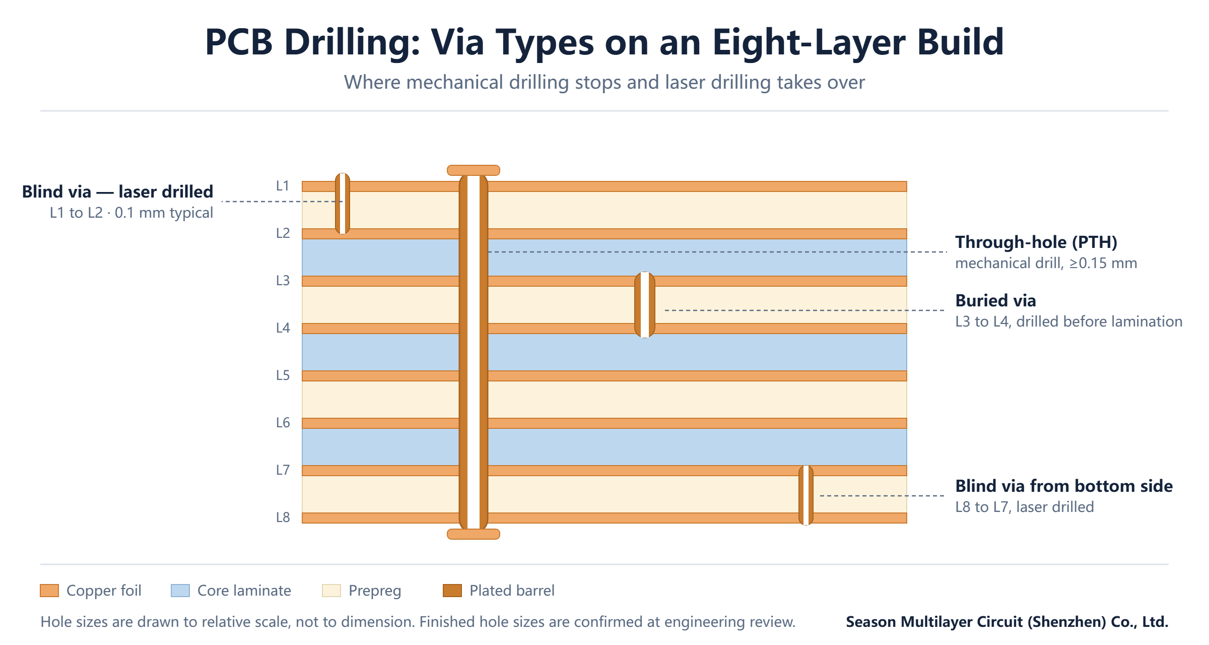
Three functional via types, plus the laser microvia, cover almost everything a buyer will specify. The differences are about span — which layers a hole connects — and that span determines which drilling technology and which process sequence apply. Getting the via type right in the data is the single most consequential drilling decision a designer makes, because it decides lamination cycles, plating requirements and cost at once.
| Via type | Spans | Formed by | Typical finished diameter |
|---|---|---|---|
| Through-hole (PTH) | All layers, top surface to bottom surface | Mechanical drilling after final lamination | 0.15 mm and above |
| Blind via | An outer layer to an adjacent inner layer | Laser drilling in HDI builds; controlled-depth mechanical drilling on conventional builds | 0.1 mm laser; 0.15 mm and above mechanical |
| Buried via | Inner layers only, never reaching the surface | Mechanical drilling of inner cores before lamination | 0.15 mm and above |
| Laser microvia | One dielectric layer per formation, in sequential build-up | UV or CO2 laser drilling on each HDI stage | 0.076–0.1 mm, confirmed per engineering review |
Two of these types interact with HDI construction choices that deserve their own reading: how microvias are arranged on top of each other. Our comparison of stacked vs staggered via structures in HDI covers that decision in depth, including why staggered arrangements are usually more forgiving in production.
Why Drilling Quality Decides Board Reliability
Electrically, a via is only as good as its plated barrel. The barrel copper bonds to the hole wall, so the wall’s smoothness and cleanliness decide adhesion; a rough or smear-contaminated wall invites voids and barrel cracking under thermal cycling, and a void in a high-current barrel is a latent field failure. This is why hole-wall quality is treated as a first-class inspection parameter rather than a cosmetic one.
The same hole also does mechanical, thermal and signal work. Mounting holes anchor connectors and hardware; arrays of vias act as thermal paths that spread heat away from power devices; and on high-speed boards, the via stub and barrel geometry directly shape impedance discontinuities and return-current behavior. Workmanship expectations for all of these are codified in the fabrication acceptance standards maintained by the Global Electronics Association, which is why class 2 and class 3 builds specify drilling-derived criteria explicitly. In short, drilling sits upstream of every reliability mechanism that matters in a finished board.
Mechanical Drilling: Entry Material, Backup Boards and Tool Wear
Mechanical drilling cuts through a stack — typically several panels pinned together — using carbide tools at spindle speeds in the six-figure rpm range. Entry material on top and a backup board underneath are part of the process, not accessories: the entry sheet centers the tool as it engages, reduces burring at breakout, and dissipates heat; the backup board protects the machine table, prevents exit burrs from tearing, and keeps the drill tip’s temperature and flute clean.
The parameter set — spindle speed, feed rate, and retract — is tuned per stack and per hole diameter, and the tool itself is a consumable with a managed hit count. Modern machines track hits per bit and schedule automatic tool changes from a magazine, which is what keeps hole diameter within tolerance across a full shift.
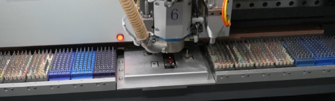
The practical floor for mechanically drilled finished holes is around 0.15 mm — below that, tool fragility, hit counts and stack height economics turn against the process, and laser drilling takes over. Aspect ratio matters too: the deeper the hole relative to its diameter, the harder uniform plating becomes, which is why high-aspect through-holes are a special-review item rather than a default.
Laser Drilling for Microvias in HDI Builds
Laser drilling forms the microvias of HDI construction. The beam ablates dielectric and stops on the copper pad beneath — contactless, with no tool to wear and no burr to remove — and it does so one dielectric layer at a time, which is why HDI boards are built in sequential lamination stages. Typical finished microvia diameter is 0.1 mm, with 0.076 mm achievable on reviewed designs; the conventional design rule keeps the blind via aspect ratio at 1:1 so the subsequent copper fill plates uniformly.
The trade-off against mechanical drilling is throughput and structure. A laser machine drills finer holes but fewer of them per hour, and each additional build-up stage adds a lamination cycle — which is why each additional HDI stage typically raises cost by 30–100% relative to the previous one. Our HDI PCB technology guide walks through the stage system in full. For a concrete production example, our 10-layer 2-stage HDI prototype PCB shows a two-stage build with laser microvias on both outer layers.

The Drilling Workflow: Before, During and After the Drill
The machine is only the middle of the workflow. Around it sit the steps that determine whether the holes come out right and whether problems get caught:
- Panel inspection and preparation — flatness, thickness uniformity and surface condition checked before anything is pinned to the table
- Drill program generation — hole positions, diameters and types compiled from the fabrication data into the machine’s NC drill file
- Parameter setup — spindle speed, feed rate and entry/backup stack configured per panel stack and hole class
- Positioning and drilling — panels located against tooling targets; registration here is what layer-to-layer accuracy inherits
- Deburr and cleaning — edge burrs and drilling debris removed so the hole wall is ready for metallization
- First-article and in-process inspection — hole diameter, position and wall quality verified with calibrated measurement before the batch proceeds
- Records — parameters, tool usage and findings archived so every subsequent batch traces to a known setup
After the drill, the hole wall is still an insulator — the next wet-process steps make it conductive. Our guide to electroless copper deposition covers exactly what happens to the drilled wall next. For where drilling sits in the full production chain from lamination to final inspection, see our multilayer PCB manufacturing capability overview.
Drill Accuracy, Hole-Wall Quality and Speed Trade-offs
Accuracy decomposes into three measured quantities: diameter (the finished hole against its specified size), position (the hole center against its nominal coordinate), and perpendicularity (the hole axis against the panel normal). All three drift with machine calibration and tool condition, which is why serious shops run scheduled machine calibration and manage tool hit counts as a controlled parameter rather than a habit.
Hole-wall quality is the second axis. A smooth, clean wall plates uniformly and bonds well; a rough or heat-damaged wall traps debris and plating solution, seeds voids, and weakens the barrel. Cutting speed is the lever with the most trade-off: too fast, and friction heat and tool wear rise together, roughening the wall; too slow, and throughput collapses without quality benefit. The optimum is a per-stack setting, which is again why the parameter record matters. Class 2 and class 3 acceptance expectations for these attributes are set out in the IPC fabrication standards published by the Global Electronics Association.
For the downstream consequence of position accuracy, our article on layer-to-layer registration accuracy connects drilling alignment to the finished board’s layer stack tolerance.
Common PCB Drilling Process Defects and How to Prevent Them
Drilling defects cluster into a small set of recurring patterns, and each has a known cause-and-prevention pair. The table lists the four that account for most of what engineers see in first-article review:
| Defect | Typical root cause | Prevention |
|---|---|---|
| Hole diameter out of tolerance | Worn tooling or feed/speed parameters mismatched to the stack | Managed hit counts with scheduled tool changes; parameter review per stack and hole class |
| Burrs and rough hole walls | Dull bits, excessive feed rate, or an unsuitable entry/backup stack | Fresh tooling at tuned feed rates; correct entry material and backup board for the panel type |
| Hole position shift | Registration error between panel and machine datum | Tooling-target alignment, scheduled machine calibration, controlled layer-to-layer registration |
| Excess drilling debris and smear | Insufficient vacuum or coolant, or an over-speed cut | Vacuum clearance at the spindle, coolant management, drilling speed held inside the qualified window |
Notice the pattern in the prevention column: every entry is a process-control measure, not a machine feature. When a supplier describes how they manage tool hit counts and parameter records, they are — indirectly but reliably — describing how your hole walls will look under cross-section.
How to Specify Drilling in Your Fabrication Drawing
Most drilling surprises trace back to ambiguity in the fab drawing, and the fix costs a few lines of text. Make these explicit:
- Finished hole sizes — state final plated diameter, letting the fabricator set tool compensation
- Via type per net class — which holes are through, blind, or buried, and which nets they may carry
- Plated vs non-plated — PTH and NPTH designations called out unambiguously
- Hole-wall plating class — the barrel thickness class the application requires
- Tent, plug or fill — which vias are covered, plugged, or filled and capped (fill decisions interact with assembly, so flag them early)
- Aspect-ratio limits — the maximum depth-to-diameter your design intends, so high-aspect holes get reviewed rather than discovered
Fill decisions deserve a second look: filled vias that support component mounting need a defined fill material and capping plan, which our article on copper-filled vias and via filling explains. For a fully documented production example of a drilled multilayer build, our 12-layer 1-stage HDI core board PCB shows how drill classes, blind vias and buried structures are specified together.
Frequently Asked Questions
What is the PCB drilling process?
It is the step in which CNC machines or laser systems cut holes into the panel: plated conduction holes for layer-to-layer interconnect and non-plated holes for mounting. It covers through-holes, blind vias, buried vias and, in HDI builds, laser-drilled microvias — and it is the foundation every later interconnect step builds on.
What is the difference between mechanical and laser PCB drilling?
Mechanical drilling cuts with a rotating carbide tool through a panel stack — versatile and fast, with a practical floor near 0.15 mm finished holes. Laser drilling ablates material with a focused beam — contactless, burr-free, and capable of 0.076–0.1 mm microvias, but slower per hole and used mainly for blind vias in HDI construction.
How small can drilled holes in a PCB be?
Mechanically drilled finished holes reach about 0.15 mm routinely. Laser-drilled microvias typically run 0.1 mm, with 0.076 mm achievable on designs reviewed case by case. Below those levels, aspect ratio, plating uniformity and cost need engineering review before a design commits.
What are blind and buried vias in PCB drilling?
A blind via connects an outer layer to an adjacent inner layer and is drilled from one surface only. A buried via connects inner layers to each other and never reaches the surface — it is drilled into the inner cores before lamination. Both differ from a through-hole, which spans the full stack and is drilled after final lamination.
Why do PCB manufacturers use entry and backup boards?
Entry material on top centers the spinning tool as it engages, reduces burring at breakout and carries heat away; the backup board underneath protects the machine table, prevents exit-burr tearing and keeps the drill tip cool and clean. Together they stabilize hole-wall quality across the whole stack.
What causes drilling defects like burrs and rough hole walls?
The usual causes are dull tooling past its hit count, feed or speed parameters mismatched to the stack, and an unsuitable entry/backup combination. Prevention is process control: scheduled tool changes, per-stack parameter records, correct entry and backup materials, and first-article inspection before a batch proceeds.
How does drilling quality affect high-speed signals?
On high-speed boards, via geometry shapes impedance discontinuities, and hole-wall roughness adds conductor loss along the barrel. A drilled hole with correct diameter, minimal stub and a smooth, well-plated wall keeps the discontinuity predictable — which is why impedance-controlled builds specify via geometry and hole quality explicitly.
Have Your Drill Data Reviewed Before Release
Drill files reward a second pair of eyes: via spans, aspect ratios and fill decisions are cheapest to review before lamination and most expensive to discover after it. Our engineering team reviews drilling data as part of every pre-quote stackup review.
Submit your Gerber and drill data through our PCB manufacturing services page — from 2 to 30 layers, with HDI and laser microvia capability confirmed per engineering review.