Book Appointment Now

A plain-English guide to PCB photoresist: how it forms circuit patterns, dry film vs liquid resist, and what buyers should check.
PCB Photoresist Explained: How Circuit Imaging Actually Works
Ask five suppliers what really limits their minimum trace width and the answers converge on one material: the photoresist. PCB photoresist is the light-sensitive film that carries your circuit artwork through exposure, development, etching and plating, and it quietly decides whether a fine-pitch design comes out as drawn or as a necked-down, marginal trace. This guide explains what it is, how the imaging sequence runs, and where it shows up in the boards you buy.
It is written from the manufacturing side — the same sequence our lines run on every multilayer job — translated into checks a hardware engineer or buyer can actually use. If two factories quote the same line and space capability but deliver different yields, how each one handles this material is usually the reason.
Table of Contents
- What PCB Photoresist Is and Why It Matters
- From Wafer Lithography to the PCB Imaging Line
- Dry Film vs Liquid Photoimageable Resist
- Positive vs Negative Working Photoresist
- PCB Photoresist in the Imaging Line, Step by Step
- How Photoresist Sets Your Minimum Trace and Space
- Where Imaging Quality Shows Up in the Finished Board
- Choosing a Resist System: Six Buyer Checkpoints
- How We Qualify the Imaging Process Before Release
- FAQ
- Have Your Imaging Windows Reviewed Before Release
What PCB Photoresist Is and Why It Matters
PCB photoresist is a light-sensitive material whose solubility changes after exposure to ultraviolet light. Coated or laminated onto the copper before imaging, it records the artwork: after exposure through a film tool and development, it remains exactly where the circuit pattern needs protection, and nowhere else. Industry literature calls the same family photoimageable resist, and it plays this template role not only in circuit board work but in semiconductor wafer fabrication and flat panel display production as well.
Four components do the work. A resin forms the backbone and provides mechanical strength and chemical resistance; a photoinitiator or sensitizer absorbs the light and starts the reaction; solvents keep liquid resists flowing for coating; and additives tune coating uniformity, light absorption and shelf stability. Dry film resists trade most of the solvent for a solid, supported sheet.
Buyers meet the property list as capability claims: sensitivity to defined wavelengths (g-line at 436 nm and i-line at 365 nm among them), resolution, resistance to etching and plating chemistries, adhesion to copper, and a process window wide enough for stable production. Every fine-line number on a quotation traces back to these properties, which is why a serious conversation about PCB photoresist is really a conversation about yield. The surface it adheres to matters just as much — our PCB materials and laminates guide covers that half of the system.
From Wafer Lithography to the PCB Imaging Line
Photoresist was born in semiconductor lithography. Bell Laboratories applied the first photoresist processes to transistor fabrication in the 1950s; negative-working cyclized rubber systems dominated early integrated circuits; and from the late 1970s positive diazoquinone–novolac resists took over as geometries shrank, because they resolve finer lines without swelling during development. Chemically amplified resists followed for deep-ultraviolet exposure at 248 nm and 193 nm, improving sensitivity by a factor of ten to one hundred, and extreme ultraviolet resists at 13.5 nm now carry the most advanced nodes. Lithography consumes roughly a third of the cost of making a chip.
Circuit board imaging borrows the physics at a friendlier scale. Wafer features are measured in nanometers; circuit board features run from a few hundred micrometers down to around fifty, and exposure units work in near-ultraviolet bands rather than deep-ultraviolet steppers. What transfers across is the logic — sensitize, expose through a mask, develop — and so do the failure modes: underexposure, incomplete development and adhesion loss look the same at any scale.
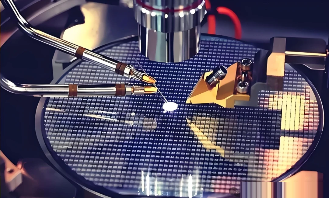
The scale difference is the point. Semiconductor resists are purified to parts-per-billion metal levels; circuit board resists are engineered for throughput and robustness on panels measured in square meters. Knowing which discipline a supplier’s capability claims come from keeps comparisons honest.
Dry Film vs Liquid Photoimageable Resist
Two formats dominate circuit board work. Dry film resist arrives as a supported solid sheet and is laminated onto the panel under heat and vacuum pressure; it is negative working and has been the outer layer workhorse for decades. Liquid photoimageable resist — LPI — is coated as a liquid, dried, then exposed and developed the same way. Both record artwork; they differ in how they reach the panel and what they tolerate afterward.
| Attribute | Dry film resist | Liquid photoimageable resist (LPI) |
|---|---|---|
| Application | Vacuum-laminated solid sheet | Curtain- or spray-coated liquid, then dried |
| Working mode | Negative (exposed areas remain) | Negative or positive, by chemistry |
| Best suited for | Standard multilayer imaging and plating masks | Features below roughly 100 µm and automated high-volume lines |
| Conformability | Follows stepped or textured surfaces under vacuum | Excellent on very flat, highly automated lines |
| Process overhead | Laminator, exposure, developer | Coating equipment, drying ovens, developer |
The practical selection logic runs by feature class and surface topography. Dry film conforms well under vacuum and strips cleanly, which keeps it attractive for standard multilayer builds; LPI earns its extra coating equipment where features push below roughly one hundred micrometers or where automated high-volume lines justify the ovens and coating hardware. The relative cost crossover moves with volume, not with any single order.
Positive vs Negative Working Photoresist
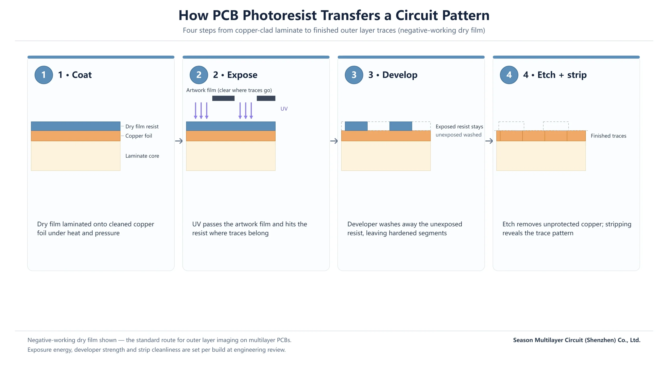
Negative resists cross-link under ultraviolet light: exposed areas become insoluble and remain after development, forming the protective pattern. Positive resists work in reverse — exposure makes the film soluble, so development removes exactly the areas the light touched. Negative chemistry pairs naturally with dry film because it is robust, fast and forgiving on production floors; positive chemistry dominates semiconductor lithography because it resolves fine geometries without the swelling that limits negative systems.
| Behavior | Negative working | Positive working |
|---|---|---|
| Reaction under UV | Cross-links and becomes insoluble | Photosensitized and becomes soluble |
| What remains after development | The exposed areas | The unexposed areas |
| Pattern vs artwork | Pattern matches the mask openings | Pattern is the inverse of the mask openings |
| Strengths | Adhesion, chemical and plating resistance, fast throughput | Resolution and clean profiles without swelling |
| Typical circuit board use | Dry film imaging and plating masks | Specialty fine-feature applications |
For a buyer the takeaway is simple: when a circuit board supplier talks about photoresist for outer layers, it is almost always negative-working dry film, and the artwork film is prepared accordingly. What matters in the quotation is not the chemistry name but the proof behind it — line width held in specification, development without residue, and clean stripping before the next step.
PCB Photoresist in the Imaging Line, Step by Step
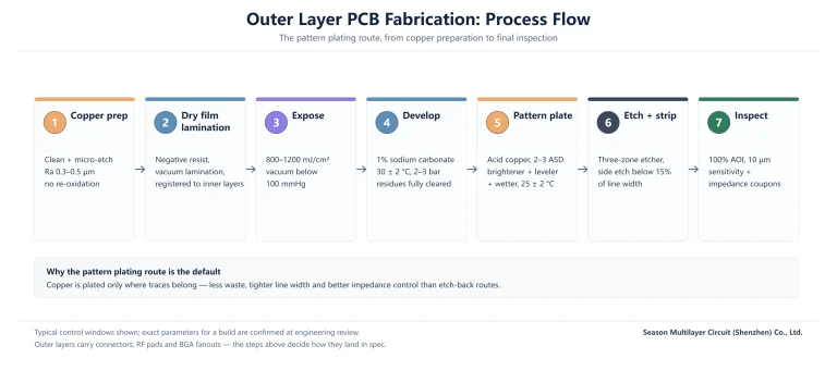
The imaging sequence is short and unforgiving. Clean copper is micro-etched so the resist can grip; dry film is laminated under heat and pressure; the panel is exposed through artwork film in a vacuum frame; and the developer dissolves the areas that must not remain. From that point the resist works for a living — as an etch mask protecting the traces being formed, or as a plating mask defining exactly where copper may grow — before the strip bath retires it.
| Step | Purpose | What the line controls |
|---|---|---|
| Clean and micro-etch | Remove oxide and roughen copper for adhesion | Chemistry strength, rinse quality, time to next step |
| Laminate dry film | Apply the photoimageable resist under heat and pressure | Roll temperature, speed, pressure, alignment |
| Expose | Transfer the artwork into the resist | Exposure energy, vacuum contact, artwork registration |
| Develop | Dissolve the areas that must not remain | Solution concentration, temperature, spray pressure, break-point control |
| Serve as mask | Protect traces during etching or define where plating grows | Resist integrity, overhang, plating uniformity |
| Strip | Remove the resist once its job is done | Chemistry strength, temperature, surface cleanliness |
| Verify | Confirm the transferred pattern | AOI coverage, line width sampling, cross-section coupons |
Every step owns a control window: laminator roll temperature and speed, exposure energy and vacuum contact, developer concentration and temperature, strip chemistry strength. When a lot fails at electrical test, the failure map usually points back to one of these windows drifting — which is why the companion question to any capability claim is how the supplier keeps those windows in control, not just what the brochure says.
How Photoresist Sets Your Minimum Trace and Space
Resolution is a chain, and the resist is one link in it. The artwork film defines the theoretical pattern; exposure optics and vacuum contact decide how faithfully light reaches the resist; the resist’s own resolution and thickness decide what survives development; and the etch or plating step adds its own geometry changes on top. A thin, high-resolution resist records fine detail but may lack the overhang a plating mask needs — thickness is a trade, not a maximum.
Our production numbers for this chain are 2/2 mil line and space on standard multilayer builds, with 1.8/1.8 mil available on samples after engineering review — verified by AOI and cross-section, not asserted. On HDI builds the same chain governs the outer layers that fan out from the microvias; see the 10-layer 2-stage HDI prototype or the 10-layer HDI industrial control PCB for how those numbers appear in a released stackup.
Where Imaging Quality Shows Up in the Finished Board
Resist problems do not stay in the imaging department. Undercut and necking trace back to exposure and development latitude; opens and shorts between neighboring features trace back to development residue or stripped adhesion; plating nodules and thin spots trace back to a plating mask that was imperfectly defined. Even solder mask — a different, permanent photoimageable layer — depends on the same imaging discipline on the surface left after etch.
The electrical consequence is impedance. Trace geometry variation shifts the impedance a high-speed line presents, which is why imaging consistency sits upstream of the impedance classes we commit to: ±10%, ±8% or ±5% depending on the build class. And because resist adhesion starts at the copper surface, the laminate system in the stackup matters too — the laminate selection guide covers how material choices interact with surface preparation.
Choosing a Resist System: Six Buyer Checkpoints
- Feature class first: name the narrowest trace and space and the smallest pad the design actually needs, not the class a datasheet brags about.
- Duty of the mask: etch protection and plating definition load the resist differently — confirm which one the build needs.
- Surface reality: stepped copper, heavy roughness and large panel size all stress lamination conformability.
- Stripping and rework: ask how cleanly the resist releases and what the surface looks like for the next step.
- Volume economics: the relative cost between dry film and liquid systems flips with automation and batch size, not with a single order.
- Evidence over adjectives: require AOI records and cross-section coupons from the actual panel, not a capability sheet.
Run any quotation through those six and the differences between suppliers stop being marketing. The supplier who answers with numbers and documents is the one whose fine-line claims will survive first articles.
How We Qualify the Imaging Process Before Release
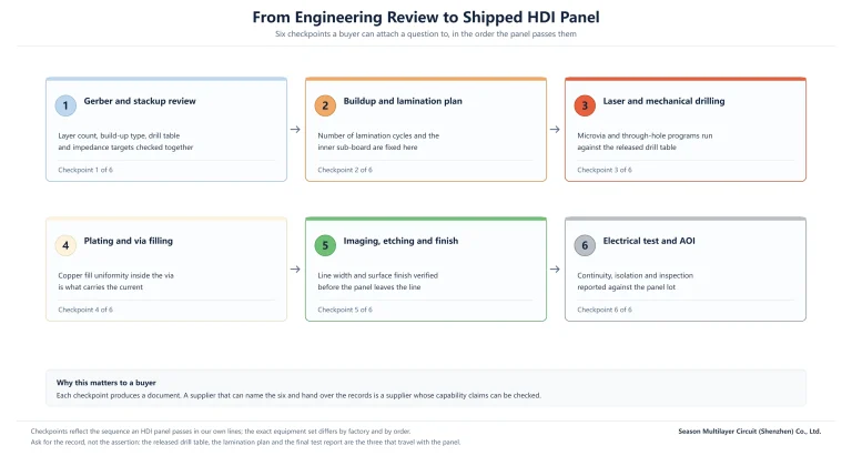
Before a new build reaches the imaging line, engineering review reads the design data as a manufacturing document — the Gerber data, the drill table and the stackup are reconciled against the impedance targets, and the artwork polarity is confirmed against the resist chemistry in use. First-article panels then carry coupons through the full sequence, and line width is measured on cross-sections rather than inferred.
Acceptance criteria follow the IPC standards — IPC-A-600 Class 2 as the default, Class 3 where the application demands it — and AOI screens one hundred percent of outer layers with defect sensitivity down to ten micrometers. Those two documents, the cross-section report and the AOI record, are the evidence a buyer should ask to see.
Everything above is how our own imaging lines run, from prototype quantities through production. If a supplier cannot produce the records, the resist was probably fine — the process discipline around it was not.
Frequently Asked Questions
What is PCB photoresist?
It is a light-sensitive film, laminated or coated onto the copper before imaging. After ultraviolet exposure through artwork film and development, it remains only where the circuit pattern needs protection from etching, or defines where plating may grow. Dry film formats dominate outer layer work, and the resist is stripped once its job is done, before surface finish and solder mask.
Does photoresist stay on the finished PCB?
No. It is a temporary process material. After etching or pattern plating, the resist is stripped chemically and the panel is prepared for solder mask and surface finish. Any residue left behind would cause adhesion and reliability problems, which is why strip completeness is a controlled step with its own inspection.
What is the difference between dry film and liquid photoresist?
Dry film is a solid sheet vacuum-laminated onto the panel; liquid photoimageable resist is coated, dried, then imaged. Dry film is the standard for multilayer outer layers because it conforms under vacuum and strips cleanly. Liquid systems suit features below roughly 100 µm and high-volume automated lines, at the cost of coating and drying equipment.
Why does PCB manufacturing prefer negative photoresist?
Negative dry film cross-links on exposure and holds up through acidic etching and acid copper plating, with strong adhesion and fast throughput. Those properties fit panel-level production better than positive chemistry, whose resolution advantage matters most at semiconductor geometries. Positive resists appear in circuit board work mainly in specialty fine-feature applications.
How does photoresist affect minimum trace width?
It is one link in the resolution chain: artwork, exposure fidelity, resist resolution and etch geometry combine to set the limit. Thinner resists resolve finer but may lack the overhang a plating mask needs. Our production capability is 2/2 mil line and space, with 1.8/1.8 mil on samples, verified by AOI and cross-section on first articles.
Is solder mask the same as photoresist?
Both are photoimageable — imaged by exposure and development — but they play different roles. Solder mask is a permanent protective layer that stays on the board; photoresist is a temporary mask used to form the circuit pattern and removed before shipment. The chemistries, thicknesses and acceptance criteria differ accordingly.
How can I verify a supplier’s imaging capability?
Ask for evidence tied to your part: the first-article cross-section report showing line width and etch profile, the AOI record for the outer layers, and which IPC acceptance class the lot was judged against. A capable supplier produces these on request; the same numbers in a brochure mean little without them.
Have Your Imaging Windows Reviewed Before Release
Send your Gerber package, drill table and impedance targets before you commit a build. Our engineering review confirms the imaging class, flags trace and space features that stress the resist window, and returns a stackup proposal with the capability numbers you can hold us to.
Start through our PCB manufacturing services page — prototype and production multilayer work, 2–30 layers, with the review evidence described above attached to your order.