Book Appointment Now

What PCB panel cutting covers before inner layers start: how units become sets and panels, and which sizing decisions decide material utilization.
PCB Panel Cutting Explained: Unit, Set and Panel Sizing Basics
Every multilayer PCB starts out as a large copper-clad laminate sheet, and the first physical step inside the factory is cutting that sheet into working panels. It sounds trivial next to laser drilling or impedance control, yet the decisions made before a single line is etched quietly set your material utilization, your effective cost per board and how smoothly production runs downstream. When quotes for the same Gerber data differ noticeably between fabricators, PCB panel cutting choices are one of the hidden reasons.
This guide explains the process from a buyer’s point of view: the difference between a unit, a set and a panel; how standard laminate sheet sizes constrain what fits; where edge rails, tooling holes and fiducials go; the utilization math that moves your price; why grain direction limits how boards can be nested; the tolerances that matter at the cutter; and what to specify when you send a design out for quotation.
Table of Contents
- What Is PCB Panel Cutting — and Why It Comes First
- Unit, Set and Panel: Three Sizes You Need to Tell Apart
- Standard Laminate Sheet Sizes and How Panels Fit Them
- Edge Rails, Tooling Holes and Fiducials
- PCB Panel Cutting Utilization: The Math That Moves Your Price
- Grain Direction, Warp and Why Cut Orientation Matters
- Cutting Tolerances, Burr and Edge Quality
- What to Send Your Fabricator: Files and Preferences That Speed Up Panel Cutting
- PCB Panel Cutting Decisions That Reach All the Way to Assembly
- Common Panel Cutting Mistakes and How to Avoid Them
- FAQ
- Have Your Panel Layout Reviewed Before the First Cut
What Is PCB Panel Cutting — and Why It Comes First
PCB panel cutting is the step that converts raw copper-clad laminate into the working panels a production line can actually process. The name emphasizes the physical cut, but the cut is the easy part. Before a blade touches material, a CAM engineer has to review the incoming Gerber data, arrange customer units into a set, group sets into a panel, and size that panel so it fits both the laminate sheet and every machine that will touch it afterwards.
It comes first for a simple reason: errors here propagate into everything after. A panel that is sized wrong forces re-nesting mid-production, changes copper distribution across the sheet, disturbs plating uniformity and can even shift where tooling holes land relative to your board features. A well-planned panel, by contrast, rides through imaging, etching, plating, lamination and assembly without a single rework loop. That is why fabricators treat panel design as an engineering task, not a warehouse chore — the same discipline described on our multilayer PCB manufacturing capability page.
For buyers, the practical takeaway is that panel decisions are shared decisions. You are free to let the fabricator optimize everything, but the more you understand the constraints, the fewer surprises you will find in the quote and the lead time.
Unit, Set and Panel: Three Sizes You Need to Tell Apart
The vocabulary matters because each level is owned by a different decision. The unit is your board — the single circuit pattern you designed, defined by your Gerber files. Nobody else can change its outline, its hole pattern or its copper. What other people can change is how many units travel through the factory together.
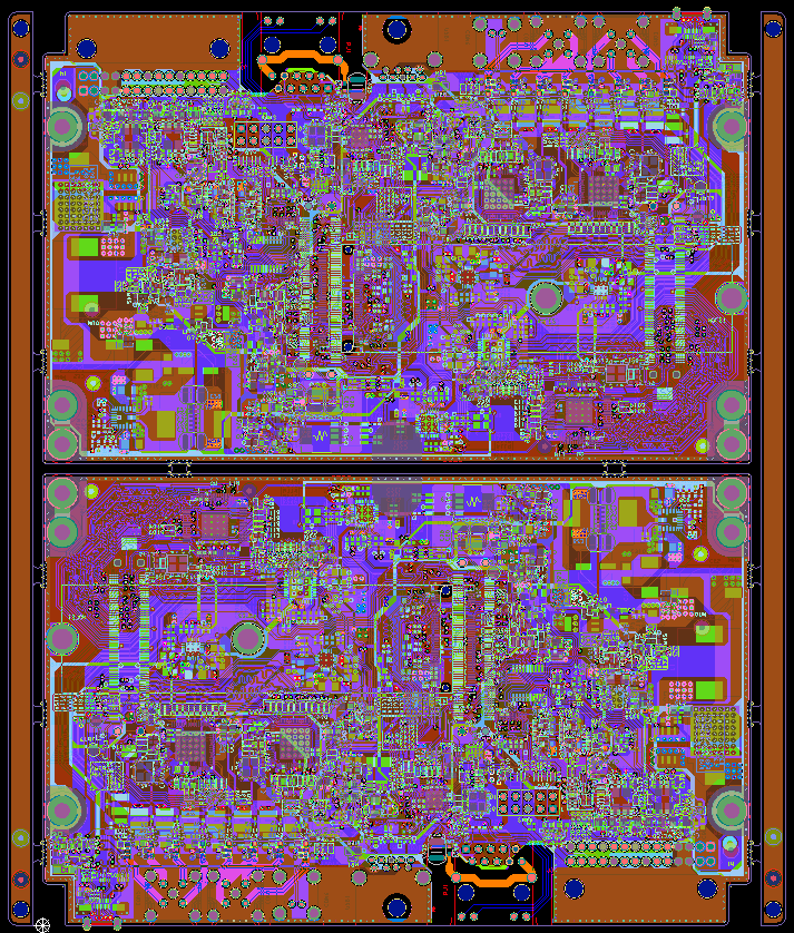
The set is a group of units arranged in a defined pattern, often with a small gap between them and a dedicated handling margin. Sets exist mainly for assembly efficiency: your SMT line runs a set through the printer and the placement machine once, then separates the boards at the end. Whether the set is designed by you or by the fabricator is a negotiation worth having explicitly, because it decides who owns the rail layout and the separation method.
The panel is the fabricator’s working board: one or more sets plus a tooling border, sized to the laminate sheet and to the equipment envelope. Several panels may be produced per sheet, and the panel is the unit that flows through drilling, plating and lamination. In short: the unit is your design, the set is your assembly convenience, and the panel is the factory’s efficiency vehicle.
Standard Laminate Sheet Sizes and How Panels Fit Them
Copper-clad laminate arrives from the material maker in a handful of standard sheet sizes — 915 × 1,220 mm and 1,020 × 1,220 mm are the most common formats a multilayer shop stages, alongside thickness- and copper-weight-specific variants. The CAM engineer’s first job is to nest panels onto those sheets with as little waste as possible, because every square millimeter of leftover edge trim is material you effectively pay for. The choice of laminate system itself — FR-4 families, mid-Tg or specialty materials — is covered separately in our PCB laminate materials guide.
| Laminate sheet size | Example panel size | Panels nested per sheet | Approx. utilization |
|---|---|---|---|
| 915 × 1,220 mm | 406 × 559 mm | 4 | ~81% |
| 915 × 1,220 mm | 305 × 406 mm | 9 | ~89% |
| 1,020 × 1,220 mm | 440 × 600 mm | 4 | ~85% |
| 1,020 × 1,220 mm | 305 × 610 mm | 6 | ~90% |
The figures above are illustrative nesting examples, not quotations — real layouts also have to respect grain direction, a feature-to-edge clearance margin, and the fabricator’s handling equipment. The pattern they show, however, is real: smaller panels nest with less waste, and a modest change in panel size can swing sheet utilization by several percentage points. Since utilization multiplies across every sheet in an order, it is one of the few purely geometric levers that reliably moves cost. Readers who want the full cost picture can see how it plays out in our PCB cost per square meter breakdown.
One more constraint hides in this step: all layers of a multilayer board must be cut from sheets with the same grain orientation, which limits how freely the nesting software can rotate panels to squeeze out waste. That constraint is important enough to deserve its own section below.
Edge Rails, Tooling Holes and Fiducials
The tooling border — usually called the edge rail — is the strip of blank laminate that surrounds your set on the panel. It is not wasted space; it is the infrastructure every downstream process hangs onto. Automated lines grip the rails to move the panel, drilling machines and exposure systems locate it by tooling holes, and optical systems align to fiducial marks placed on it.
- Tooling holes for pin-based lamination and mechanical registration in drilling and routing
- Global fiducial marks for camera alignment at exposure, AOI and assembly
- Space for test coupons, when the panel layout allows, so impedance and microsection checks ride along with production
- Room for fabrication markings such as date codes and certification logos, kept clear of your circuits by agreement
Rail width is a trade-off: narrow rails maximize utilization but give automated handlers less to grip, while wide rails are robust and waste copper. A typical working range is 5–10 mm per side, with the exact value chosen to match the shop’s conveyor and pin systems. Anything placed on a rail — including coupon circuitry — is copper the fabricator etches and then discards, which is why rail content is agreed at engineering review rather than improvised.
PCB Panel Cutting Utilization: The Math That Moves Your Price
Utilization is simply the share of the sheet that ends up as shipped copper. It is the cleanest illustration of why panel design is an economic decision. Take a 100 × 80 mm unit and compare three nesting strategies, holding the edge rail at 10 mm and the unit gap at 5 mm:
| Arrangement on the sheet | Working panel size | Units per panel | Utilization |
|---|---|---|---|
| Single unit with 10 mm edge rails | 120 × 100 mm | 1 | 67% |
| 2 × 2 set, 5 mm unit gap, 10 mm rails | 225 × 185 mm | 4 | 77% |
| 3 × 4 set, 5 mm unit gap, 10 mm rails | 330 × 355 mm | 12 | 82% |
The 3 × 4 arrangement consumes roughly 23% less laminate per board than the single-unit panel — and laminate is only the beginning, because fewer panels also mean fewer handling cycles, fewer drill loads and less chemistry per unit. Fabricators do not pass every gain straight through to the quote, since process constraints (panel size limits per layer count, copper balance, plating uniformity) cap how far nesting can go, but the direction of the effect is never in doubt.
The buyer’s move is to ask the question early: if your volumes justify it, ask whether your design nests efficiently and whether a small outline or array change would materially improve the number. Reputable fabricators run this analysis during design-for-manufacturing review and will tell you plainly.
Grain Direction, Warp and Why Cut Orientation Matters
Woven glass reinforcement gives laminate a grain — a machine direction and a cross direction with slightly different stiffness and moisture response. Panels cut with their long axis along the machine direction behave more predictably through the heat of lamination and assembly; panels mixed in both directions fight each other inside the stackup. That is why PCB panel cutting is not free to rotate every nesting candidate for maximum utilization: all layers of a multilayer build must share one grain orientation.
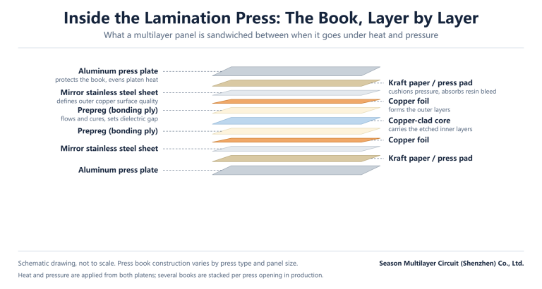
Grain control is one half of the flatness story; the other half is a copper-balanced stackup, where copper distribution mirrors around the center of the board. Both topics converge in the PCB lamination process, where mismatched grain or unbalanced copper shows up as bow and twist after the press. A warped panel is not a cosmetic problem — it jams assembly rails and lifts corners off solder paste prints.
There is also a storage dimension. Cut panels are staged in temperature- and humidity-controlled conditions, because exposed laminate edges drink moisture and copper foils oxidize. Panels that sit too long before imaging get cleaned or scrapped, which is one more reason fabricators sequence cutting close to the next process step.
Cutting Tolerances, Burr and Edge Quality
What does the cut itself have to achieve? Three things: size, squareness and edge condition. Panel dimensions are held to a tight working tolerance — typically in the ±0.2 mm class for multilayer work, confirmed at engineering review against the shop’s equipment — because the panel is the reference for every alignment operation that follows. Squareness matters for the same reason: a slightly trapezoidal panel makes camera-based alignment fight a moving target.
Edge condition matters more than buyers expect. Shearing and sawing can leave burrs and fiberglass dust on the panel edge; in subsequent wet processes, loose debris and protruding glass fibers interfere with imaging and etching, producing defects far from the cut itself. Good shops deburr and clean panels before inner-layer imaging for exactly this reason.
A related set of choices — how finished boards separate from the panel at the end of assembly — is actually designed at the cutting stage, because the array geometry has to be built in from the start:
| Separation method | Edge condition | Mechanical stress | Best suited for |
|---|---|---|---|
| V-score (V-groove) | Clean, straight edge | Moderate bending at break-out | Rectangular units in medium-to-high volume |
| Tab-routing with mouse bites | Routed outline with perforated tabs | Low | Irregular outlines and boards with component overhang |
| Solid tab, routed both sides | Smooth routed edge, tab finished after separation | Lowest | Heavy or edge-sensitive assemblies |
If your assembly partner will depanel by router, say so early: the fabricator will leave tabs where they can carry the board safely, and the two specifications will agree before anything is cut.
What to Send Your Fabricator: Files and Preferences That Speed Up Panel Cutting
Panel cutting is where file quality is first tested. CAM engineers cannot nest what they cannot trust: an outline that disagrees between the mechanical layer and the copper layers stops the job until it is resolved. Sending a complete, self-consistent data package — ideally industry-standard Gerber data plus drill files and a short fabrication note — is the single fastest way to keep this step moving. Our PCB prototyping process guide walks through the full data package from quote to first article.
- A complete outline in the mechanical layer that matches every copper layer
- Your array preference: loose units, a customer-defined set, or fabricator-optimized nesting
- Rail side and width constraints if your SMT conveyor clamps demand them
- Whether test coupons are needed, and roughly where they may sit
- The depaneling method your assembly line will use, so V-grooves or tabs are built into the array
- Layer count, material system and copper weights, so the right laminate sheets are staged before cutting
None of this needs to be perfect on the first pass — that is what the engineering review is for — but a buyer who arrives with these answers gets a panel design and a quote days earlier than one who does not.
PCB Panel Cutting Decisions That Reach All the Way to Assembly
Panel decisions made at the cutter keep surfacing after your boards leave the fabricator. The rails that carried the panel through etching become the conveyor edges your assembly line grips; the fiducials placed for exposure alignment double as placement-machine references; the tab positions chosen for depaneling determine whether components near the board edge survive separation. A panel is a supply-chain object, not just a manufacturing one.
This is easiest to see on real builds. High-density products such as our 10-layer HDI industrial control PCB carry fine-pitch components close to the board edge, so tab placement and rail width are agreed before production, not improvised at the assembly bench. Consumer boards like the 8-layer computer peripheral boards we build run high volumes where a few percentage points of panel utilization translate into meaningful annual savings. The design standards referenced in both cases — the IPC design and acceptability standards — assume panelization decisions were made deliberately.
For buyers, the checklist is short: confirm who owns the array design, confirm the depaneling method, and confirm that fiducials and rails match the assembly line’s expectations. Those three confirmations prevent most panel-related assembly surprises.
Common Panel Cutting Mistakes and How to Avoid Them
- Outline data that disagrees between mechanical and copper layers — resolved by a single source of truth for the board outline
- Asymmetric rails that fit the fabricator’s line but not the assembly conveyor — resolved by sharing SMT line constraints early
- Arrays requested without component-overhang allowance, so parts sit over the separation line — resolved by checking the placement data against tab positions
- Nesting that ignores grain direction and produces post-lamination warp — resolved by locking one orientation for all layers
- Mixing board revisions in one panel to save setup — resolved by treating every revision as its own order, however small
Every item on this list is cheaper to fix in a design review than on the production floor. Fabricators catch most of them during DFM checks, and the good ones send the panel layout drawing back for your approval before cutting — an approval step worth actually reading rather than rubber-stamping, because it is your last inexpensive chance to change how your boards are made.
From here the panels move into imaging and etching — the inner layer processes covered in our companion guide to PCB inner layer fabrication.
Frequently Asked Questions
What is PCB panel cutting in PCB manufacturing?
It is the first fabrication step: raw copper-clad laminate is reviewed, nested and cut into working panels that carry one or more copies of your design plus a tooling border. It covers the CAM work (Gerber review, set and panel design) as well as the physical cut, and it sets material utilization and downstream process alignment for the whole build.
What is the difference between a unit, a set and a panel?
The unit is your single board as defined by the Gerber data. The set is several units arranged together with a small gap, sized for efficient assembly and depaneling. The panel is the fabricator’s working board: one or more sets plus edge rails and tooling features, sized to the laminate sheet and production equipment.
How much does panel utilization affect PCB cost?
Materially. In the worked example above, moving from a single-unit panel to a 12-up panel cut laminate consumption per board by roughly a fifth, and fewer panels also mean fewer handling and process cycles. Fabricators balance utilization against plating uniformity and equipment limits, so the exact effect is quoted per design — but utilization always points the cost needle.
What are standard PCB laminate sheet sizes?
Common multilayer sheet formats include 915 × 1,220 mm and 1,020 × 1,220 mm, staged in specific thicknesses and copper weights per order. Fabricators nest panels onto whichever format wastes less material for a given design, which is why two shops can quote the same board with different economics.
Should I panelize my own boards or let the fabricator do it?
Either can work. Supply your own array if your assembly line needs specific rails, fiducials or depaneling geometry; otherwise let the fabricator optimize nesting — they know their sheet sizes, equipment envelopes and grain-direction constraints. Just state the choice explicitly so nobody redesigns the array twice.
What is an edge rail on a PCB panel?
The blank laminate border around your set, typically 5–10 mm wide, used for tooling holes, fiducial marks, coupon space and conveyor handling. Rails are consumed in production and separated before shipment, so nothing functional should be placed on them without agreement.
Does panel cutting affect warpage?
Yes, through grain direction. Laminate is stiffer along the woven glass machine direction, and panels cut with all layers sharing one orientation stay flatter through lamination and assembly. Mixing orientations inside a stackup is a classic cause of bow and twist after the press.
Have Your Panel Layout Reviewed Before the First Cut
Panel sizing is the cheapest decision in your build to change and the most awkward to discover late. Utilization, rail layout, grain direction and depaneling geometry are exactly the checks our engineering team runs when a new multilayer design arrives for quote.
Send your Gerber data through our PCB manufacturing services page — from 2 to 30 layers — and we will return a panel layout drawing you can actually read, with utilization and array options confirmed at engineering review.