Book Appointment Now

U.2 SSD PCB design explained: SFF-8639 signal groups, layer counts, 85-ohm differential routing, hot-plug power delivery and the fabrication rules that set yield.
U.2 SSD PCB Design: SFF-8639 Carrier Board Layout and Build Rules
U.2 remains the workhorse enterprise SSD interface: a 2.5-inch, hot-pluggable drive speaking NVMe over four PCIe lanes through the SFF-8639 connector. For the team building the drive – or the backplane, adapter or storage appliance around it – the U.2 SSD PCB is a study in a different trade-off than M.2: more board area, a hotter power envelope, and a connector whose pin groups dictate the fanout. This guide covers the carrier board decisions that matter, from stackup to surface finish.
The framing is engineer-to-engineer: what each SFF-8639 signal group needs from the board, how layer count follows the interface generation, where the 85 Ω differential discipline is non-negotiable, and which fabrication choices decide yield. Where a value depends on your platform, it is marked for confirmation at engineering review.
Table of Contents
- What a U.2 SSD Carrier Board Is
- U.2 vs M.2 vs E1.S: How the PCB Design Changes
- U.2 SSD PCB Stackup and Layer Count
- SFF-8639 Signal Groups and How to Fan Them Out
- Differential Impedance and the PCIe Loss Budget
- Hot-Plug, Dual-Port and Power Delivery
- Mechanical and Thermal Constraints of the 15 mm Envelope
- Fabrication Rules for U.2 SSD PCB Builds
- Where U.2 Still Fits as E1.S and E3 Grow
- FAQ
- Get Your U.2 SSD PCB Stackup Reviewed Before Layout Freeze
What a U.2 SSD Carrier Board Is
U.2 is the marketing name the SFF working group gave to the SFF-8639 specification – originally “SSD Form Factor 8639”. The connector carries SATA, SAS and PCIe signalling on one common interface, which is why a single backplane family can serve spinning-disk replacements and NVMe drives side by side. In practice, “U.2 SSD” today means a 2.5-inch drive running NVMe over PCIe x4, hot-pluggable from the front of a server.
From a board perspective the drive is a stiffened 2.5-inch PCB assembly: controller, DRAM, a large NAND field and power-loss protection capacitors, mechanically packaged for a drive bay and mated to the host through a backplane connector rather than a cable. The backplane half of the mating pair is a separate product with its own PCB requirements – many of the rules in this guide apply to both halves.
That duality is worth keeping in mind when you qualify suppliers. A fabricator who can prove controlled impedance on a drive carrier can prove it on a backplane; the difference is scale, layer count and connector mount, not signal discipline.
U.2 vs M.2 vs E1.S: How the PCB Design Changes
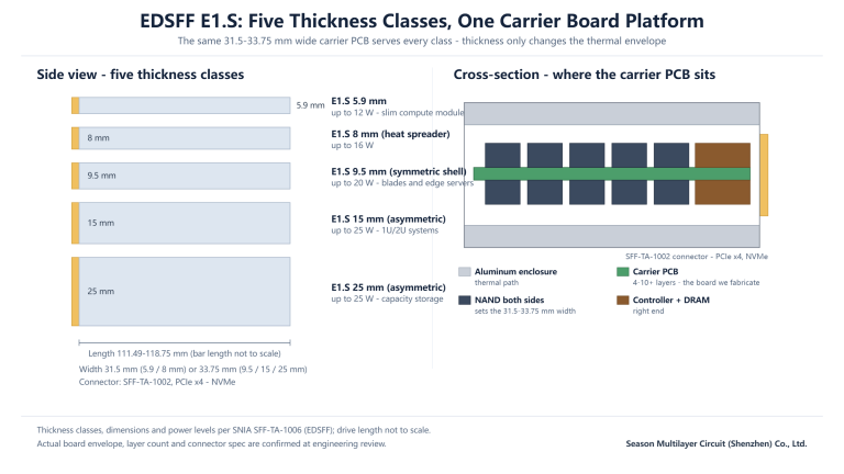
Three envelopes dominate enterprise and client storage, and each pushes the U.2 SSD PCB (and its siblings) toward different decisions. M.2 trades everything for volume: no hot-plug, tight power, a stick that lives inside the chassis. E1.S trades board area for density: a narrow vertical carrier with standardised thermals. U.2 keeps the 2.5-inch bay – the largest board area of the three – plus native hot-plug and a mature backplane ecosystem.
| Attribute | U.2 (SFF-8639) | M.2 | E1.S (EDSFF) |
|---|---|---|---|
| Envelope | 2.5-inch drive bay, 15 mm class | 22 mm wide stick, 30-110 mm long | 31.5-33.75 mm wide vertical drive, 5.9-25 mm thick |
| Connector | SFF-8639, backplane mating | M.2 edge socket on host board | SFF-TA-1002 edge fingers |
| Hot-plug | Native | Not native | Native |
| Board area for NAND | Largest of the three | Smallest | Narrow but long, both faces |
| Typical host | Enterprise servers, storage arrays | Client PCs, embedded | Hyperscale 1U front bays |
For the board designer, the practical translation: U.2 gives you room to route and to place a serious PLP capacitor bank, at the cost of managing a tri-protocol connector and a mechanical package designed for bays rather than sockets. Our E1.S SSD PCB design guide covers the EDSFF equivalent of every decision in this article.
U.2 SSD PCB Stackup and Layer Count
Because a 2.5-inch board offers roughly four times the usable routing area of an M.2 2280, layer count grows more slowly with interface speed than on narrow carriers. A 4-layer SATA SSD PCB is the classic entry point; PCIe 4.0 x4 NVMe drives typically land on 6-8 layers; PCIe 5.0 and dual-port designs push to 10 or more – the range our 10-layer USSD PCB was built for.
| Interface class | Typical carrier layers | What drives the count |
|---|---|---|
| SATA 6 Gb/s | 4-6 | Single pair, PLP bank, one-face NAND options |
| PCIe 4.0 x4 NVMe | 6-8 | Four lane pairs, eight NAND channels, power planes |
| PCIe 5.0 x4 or dual-port NVMe | 10+ | Escape density, reference planes, second port group |
Two stackup rules pay for themselves on every storage build. Keep the symmetric construction so the board stays flat through reflow with components on both faces. And dedicate at least one unbroken ground plane adjacent to every high-speed routing layer – on a tri-protocol board, the SATA and sideband routing will happily cross your PCIe return path if you let it.
SFF-8639 Signal Groups and How to Fan Them Out
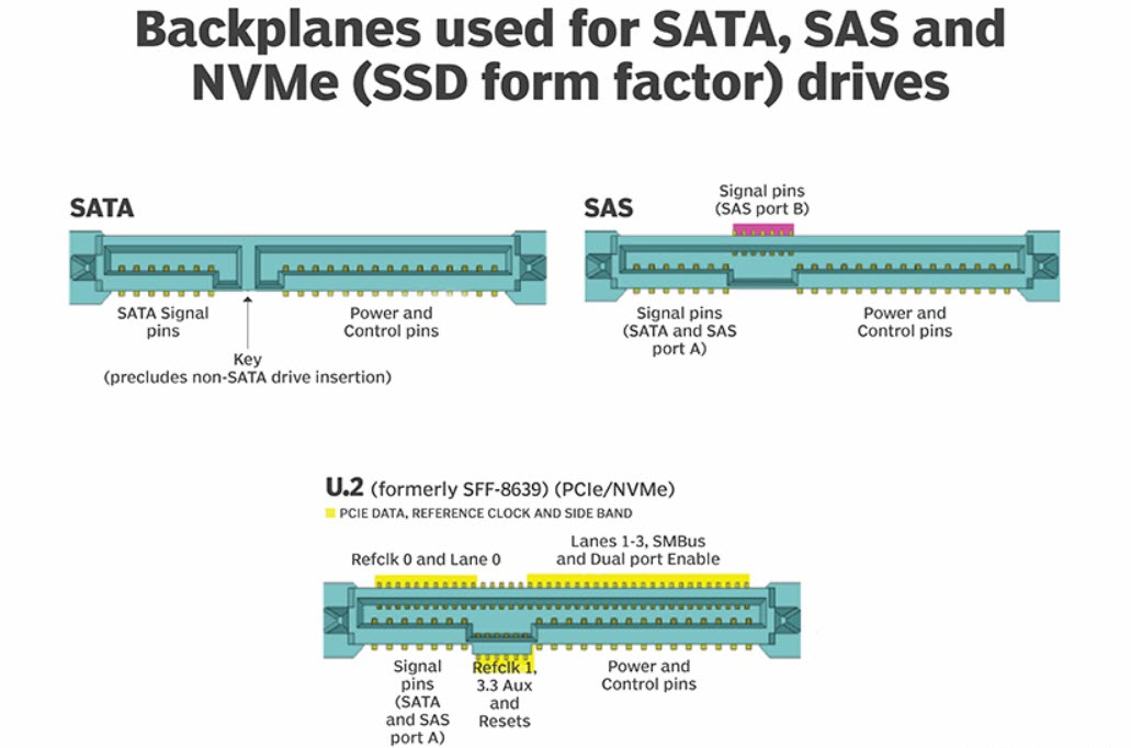
The SFF-8639 pin field is best treated as five signal groups, each with its own routing personality. The diagram above shows how the groups sit in the connector; the table translates them into board requirements. This is also where the drive-side carrier and the backplane diverge: same groups, different physical connector.
| Signal group | Function | PCB handling |
|---|---|---|
| Four PCIe lanes plus reference clocks | Host data path | 85 Ω differential pairs, length-matched, solid return planes |
| SMBus sideband and dual-port enable | Management and redundancy | Low-speed routing, keep clear of lane pairs |
| 3.3 V auxiliary and resets | Power-up sequencing | Dedicated plane region, sequenced rails |
| SATA/SAS port A group | Legacy protocol compatibility | Populated only on tri-mode designs |
| Power and control pins (12 V, 3.3 V) | Drive power | Wide pours sized for inrush, close to the PLP bank |
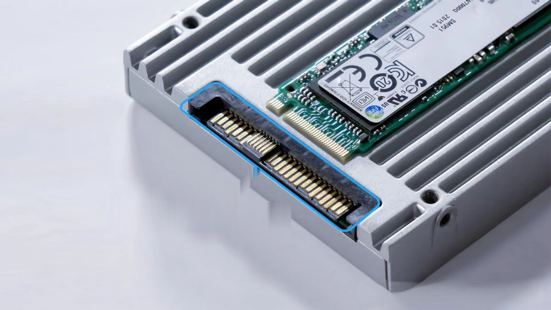
Fanout discipline: escape the lane pairs first, in the first 8-10 mm from the mating edge, and hold them together as a group. The sideband and auxiliary groups can take the scenic route, but never let a management trace split a lane pair’s return path. On the drive side, the remaining area belongs to NAND channels – which is why the controller placement usually starts from the connector end of the board.
Differential Impedance and the PCIe Loss Budget
PCIe lanes route at 85 Ω differential. Hold ±10% as your standard expectation, and reserve ±8% or ±5% for designs whose loss budget is genuinely tight – tolerance is a purchased capability, and it is priced accordingly. The U.2 channel is longer than an M.2 channel by nature: drive carrier, backplane connector, backplane traces and host board all share one insertion loss budget, so the drive-side carrier does not get a private allowance.
At PCIe 5.0’s 32 GT/s, the 16 GHz Nyquist content makes the laminate’s dissipation factor the dominant loss term. That is a material selection question first – our laminate selection guide compares the grades – and a via discipline question second: filled vias under the controller, short stubs everywhere, and no unnecessary layer transitions on lane pairs.
Hot-Plug, Dual-Port and Power Delivery
Hot-plug shapes the power design more than the signal design. The backplane connector manages pin stagger and pre-charge, but the carrier must survive the event: the PLP capacitor bank covers the load-transient dip during insertion, inrush on the 12 V rail is limited by design rather than by luck, and the 3.3 V auxiliary rail supports the sequencing the host expects. Size the power pours for the inrush case, not just the steady-state current.
Dual-port is the quiet redundancy feature of U.2: the dual-port enable sideband lets two independent hosts talk to one drive, so a path failure does not take the volume offline. On the carrier it costs a second set of lane pairs routed to the connector’s second port group – and that second group is usually what pushes a dual-port design up a layer count. Decide early whether your product claims dual-port, because retrofitting it into a single-port layout is a respin.
A note on U.3: it extends the U.2 ecosystem toward tri-mode operation, but compatibility between U.2 drives and U.3 hosts depends on which generation each side implements. Qualify the drive-plus-backplane pair rather than assuming the badge on the bay.
Mechanical and Thermal Constraints of the 15 mm Envelope
The 2.5-inch bay is a mechanical specification as much as an electrical one. The carrier needs stiffening where it meets the connector (drive-side builds often add a stiffener or metal backing at the mating edge), mounting features that match the bay, and a component height budget that clears the shell – including the PLP capacitor bank, which is routinely the tallest object on the board.
Thermally, a U.2 drive leans on its enclosure the way E1.S does: shell fins and thermal interface materials move heat to airflow, while the PCB’s copper planes spread it away from controller and NAND hot spots. The difference is area – with roughly four times an M.2’s board surface, the U.2 SSD PCB has room for generous copper pours, and using them costs nothing at layout time.
Fabrication Rules for U.2 SSD PCB Builds
Acceptance class is the first callout to get right: IPC-6012 Class 3 is the norm for enterprise storage hardware, and it changes how the fabricator inspects plating, annular ring and dielectric spacing – IPC-2226 and its sibling standards define what the class demands. Say so in the drawing; it is cheaper than arguing about it after the fact.
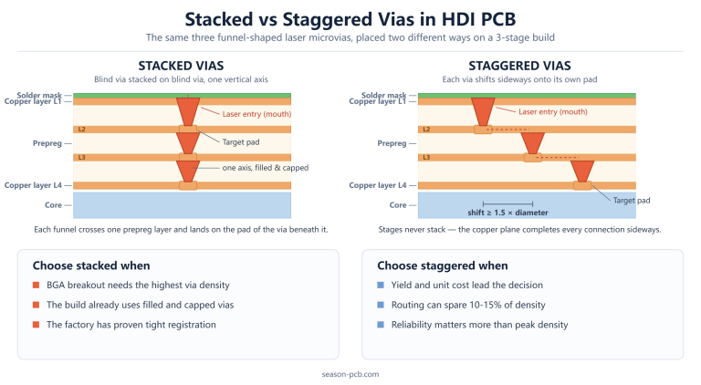
Process notes that save respins: specify ENIG or another planar finish for the BGA fields, call out filled and capped vias wherever a via shares a pad – the copper filled via process page explains why wicking and flatness matter at second-side assembly – and request controlled-impedance coupons on every panel. When the data package is ready, a reviewer who can read the Gerber data against a written stackup will catch most issues before they become boards.
Where U.2 Still Fits as E1.S and E3 Grow
EDSFF is where the new designs are heading – the E3 family was drafted explicitly to supersede U.2 in future servers – but U.2’s installed base is enormous, and tri-mode backplanes keep it relevant for mixed SAS, SATA and NVMe fleets. Form factor transitions in storage run on five-to-ten-year clocks, not product cycles.
- Choose U.2 when the platform already owns 2.5-inch bays, when capacity per drive leads the requirement, or when tri-mode protocol support matters
- Choose E1.S for new hyperscale-density builds where front-bay count and standardised thermals win
- Choose M.2 for client and embedded products where a socket on the host board beats a bay
- For any new enterprise platform, budget the E1.S/E3 evaluation now even if U.2 ships first
Whichever envelope your roadmap picks, the board-level disciplines overlap almost completely: symmetric stackups, 85 Ω differential routing, filled vias under fine-pitch parts and a PLP bank that is designed in, not squeezed in.
Frequently Asked Questions
What is a U.2 SSD?
A U.2 SSD is a 2.5-inch enterprise drive that runs NVMe over four PCIe lanes through the SFF-8639 interface. It is hot-pluggable, mates to backplanes in server bays, and comes in capacities that larger drives in the same bay class can support – which is why it remains the default choice for capacity-focused enterprise storage.
Is U.2 the same as SFF-8639?
Yes. SFF-8639 is the engineering specification name – originally “SSD Form Factor 8639” – and U.2 is the shorter marketing name the SFF working group adopted later. They refer to the same connector and interface; datasheets use the terms interchangeably.
U.2 vs M.2: which should a server design use?
Servers use U.2 when they need hot-plug serviceability, large capacity per drive and a real power envelope; M.2 when the drive lives inside a chassis next to the motherboard and volume is the constraint. U.2 carriers are bigger, thermally capable of more, and designed for bay service rather than board-level sockets.
Can a U.2 SSD be used in a U.3 backplane?
Not automatically. U.3 extends the U.2 ecosystem with tri-mode operation, but compatibility depends on which generation of the specification each side implements – a U.2 drive may not work in every U.3 host. Qualify the specific drive-backplane pair before ordering volume.
How many layers does a U.2 SSD PCB need?
Plan on 4-6 layers for SATA-class designs, 6-8 for PCIe 4.0 x4 NVMe, and 10 or more for PCIe 5.0 or dual-port products. The 2.5-inch board area relaxes escape density compared with M.2, so treat layer count as a routing calculation confirmed at engineering review.
What impedance do PCIe traces on a U.2 SSD PCB use?
85 Ω differential is the PCIe target, with fabricators holding ±10% as standard and ±8% or ±5% available for tighter budgets. Remember the channel includes the backplane: match the drive-side carrier’s impedance discipline to the host environment rather than optimising it in isolation.
Who manufactures U.2 SSD carrier boards?
Fabricators with controlled-impedance and fine-pitch assembly experience. Our factory builds storage carriers from 4-layer SATA boards to 10-layer NVMe designs under IPC-6012 Class 3 acceptance, with ENIG, filled vias and impedance coupons as standard offerings. Send your stackup for a buildability review before layout freeze.
Get Your U.2 SSD PCB Stackup Reviewed Before Layout Freeze
Send your stackup intent, SFF-8639 pin-group assignment and PLP bank plan, and our engineering team will review layer count, impedance targets and hot-plug power routing against your platform – then quote the build. Start from the PCB manufacturing services page, or reference our shipped 10-layer USSD PCB.