Book Appointment Now

Cross blind and buried via HDI staggers blind microvias against buried vias to solve thickness, clearance and cost problems that defeat through-hole layouts.
Blind and Buried Via HDI: Cross Via Structures for High-Density PCBs
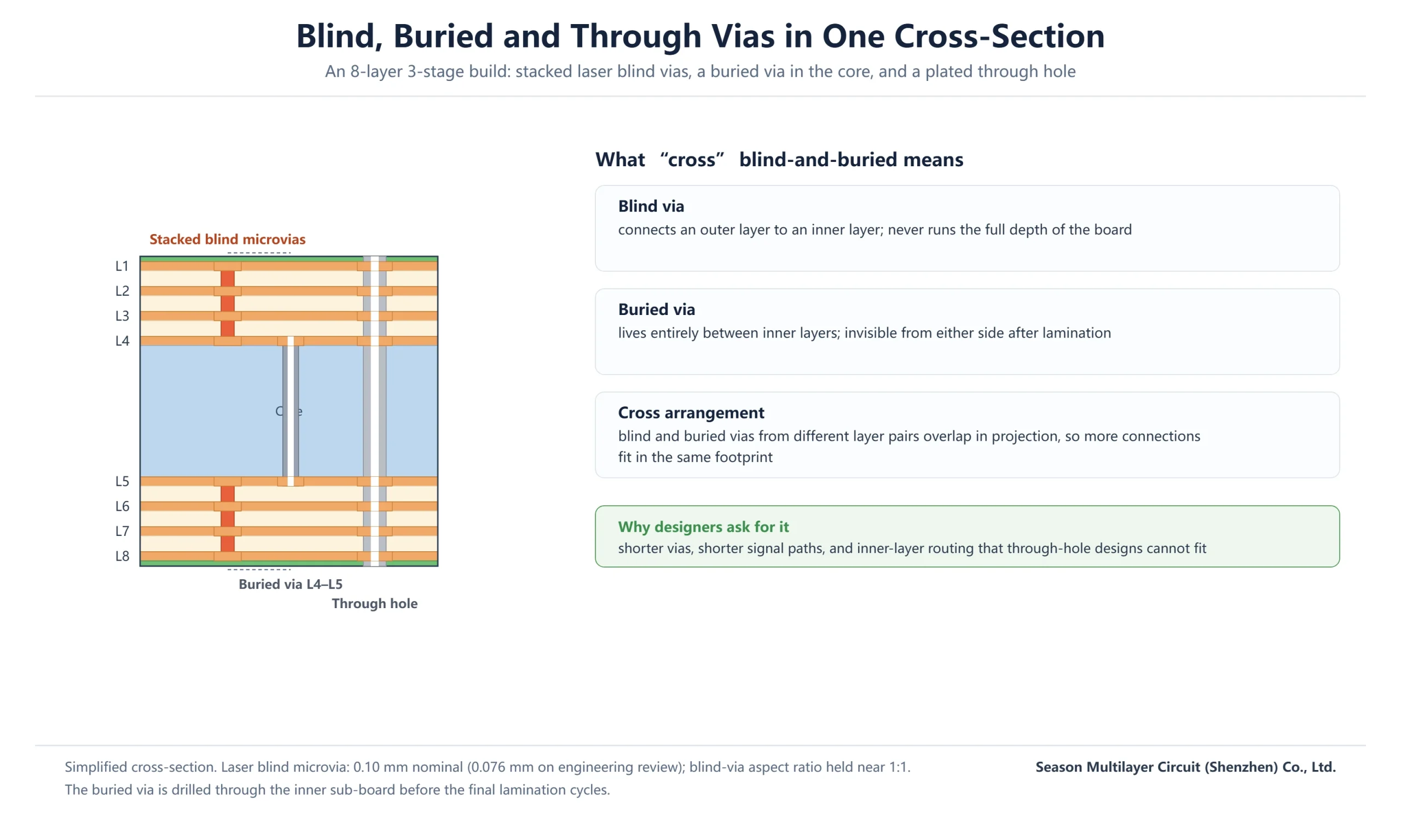
When a dense board refuses to route, the usual reflexes are to add layers or jump straight to any-layer HDI. There is a third option that engineers often meet too late: blind and buried via HDI with a cross arrangement, where blind microvias and buried vias from different layer pairs deliberately overlap in projection. That staggered structure solves three problems at once — board thickness limits, via-to-trace clearance on inner layers, and the cost of full any-layer interconnect.
This guide walks through what the structure actually is, the three problems it is best at fixing, the design rules that keep it manufacturable, and a decision table for choosing between through-hole, blind-and-buried and any-layer constructions. Everything here reflects what our engineering team checks when a conversion request arrives.
Table of Contents
- What Blind and Buried Vias Are — and What Cross Adds
- Why Through-Hole Designs Hit a Wall
- How Blind and Buried Via HDI Relieves Thickness Limits
- Fixing Via-to-Trace Clearance on Inner Layers
- Cutting the Cost of Any-Layer Interconnect
- Design and Manufacturing Rules for Cross Blind and Buried Via HDI
- Where the Structure Pays Off
- Choosing Between Through-Hole, Blind-and-Buried and Any-Layer
- FAQ
- Have Your Via Structure Reviewed Before You Quote
What Blind and Buried Vias Are — and What Cross Adds
The vocabulary has to be exact, because the three via types behave completely differently in both design and manufacturing.
| Via type | Spans | Visible from the surface | How it is made | Typical role |
|---|---|---|---|---|
| Through via | Every layer of the board | Both sides | Mechanical drilling after final lamination | Power delivery and general interconnect |
| Blind via | An outer layer to one or more inner layers | One side only | Laser drilling (or controlled-depth drilling) | Breakout and escape routing under fine-pitch BGAs |
| Buried via | Inner layer to inner layer | Neither side | Mechanical drilling of a pre-laminated sub-board | Dense inner routing without consuming surface real estate |
| Cross arrangement | Several blind and buried via pairs, overlapping in vertical projection | Varies per via | Sequential lamination with deliberately staggered placement | Interconnect density that through-hole structures cannot reach |
The word cross describes the geometry. In a conventional stack, vias from different layer pairs sit side by side so their shadows never overlap. In a cross arrangement, the designer lets them overlap in projection: a blind via on the top half of the board can sit directly above a buried via deeper in the stack, because the two never contend for the same layer. Overlapping shadows mean more interconnect per square millimetre without forcing every connection through the full thickness of the board.
That one geometric idea is what separates the structure from ordinary blind-and-buried usage, and it is the reason the rest of this article exists. Almost every benefit below — thinner allowed dielectrics, recovered clearance, lower cost than any-layer — falls out of letting vias overlap where a through hole would have blocked them.
Why Through-Hole Designs Hit a Wall
A plated through hole is wonderfully cheap and utterly greedy. It occupies every layer it passes, whether or not that layer wants the connection. Each through hole demands an anti-pad — a clearance opening — on every plane it crosses and a keep-out on every signal layer it passes. On a sixteen-layer board with thousands of holes, those clearances quietly consume the very routing channels the extra layers were added to provide.
Thickness makes the problem worse. The deeper the board, the smaller the usable drill diameter for a given aspect ratio, and the longer the unused barrel that hangs below every connection — a stub that degrades high-speed channels and adds inductance to power paths. Manufacturing, meanwhile, has to plate a hole whose wall quality degrades as depth grows relative to diameter. At some point the design cannot get thinner routes, more layers or better signal behaviour out of through-hole technology, no matter how carefully it is autorouted.
The two failure modes customers bring us most often are the direct consequences: either the routing simply does not fit because hole keep-outs strangle the inner layers, or a specific hole sits too close to an inner-layer trace and violates the electrical clearance the design needs. Both have structural answers rather than routing tricks.
How Blind and Buried Via HDI Relieves Thickness Limits
Any-layer HDI earns its name by letting every layer pair connect through stacked laser microvias. The price is that every dielectric a laser via crosses must stay thin: the laser has a practical aspect-ratio window, so the material between two layers joined by a stacked laser via cannot simply be thickened when the impedance stackup or the copper weights demand it. Designers end up fighting the stackup calculator against the laser process window.
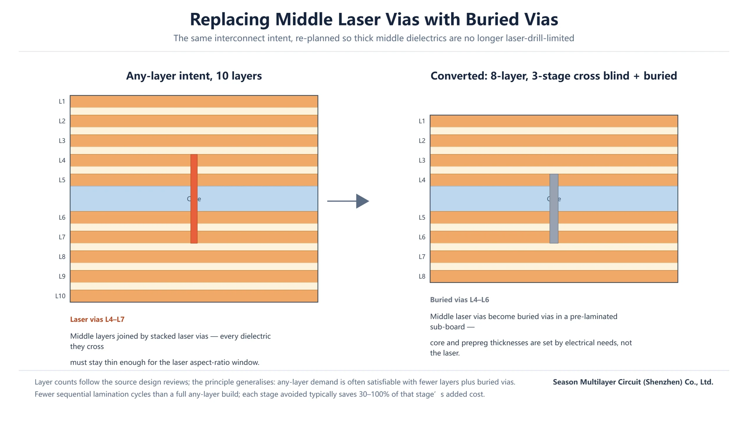
The cross structure breaks that deadlock. Take a ten-layer any-layer intent whose middle layers are chained by stacked laser vias. Converting those middle laser vias into buried vias — drilled through a pre-laminated sub-board before the final lamination cycles — removes them from the laser process window entirely. The core and the prepreg layers around the buried-via region can then be thickened to whatever the electrical design needs, because a mechanical drill on the sub-board handles those depths comfortably. In one reviewed conversion of this kind, a ten-layer any-layer intent became an eight-layer, 3-stage HDI construction with the same interconnect plan and none of the middle-dielectric restriction.
There is a signal-integrity bonus. Vias that span only the layers they need are shorter than through holes doing the same job, so the stub either shrinks or disappears. Shorter barrels mean less unused metal in the path, cleaner high-frequency behaviour and a little more routing freedom around every connection. For designs carrying multi-gigabit channels, that alone can justify the conversion.
Fixing Via-to-Trace Clearance on Inner Layers
Hole-to-line clearance failures are less dramatic than routing failures but just as fatal at design review. A hole that passes an inner signal trace too closely invites crosstalk, and in the worst case a breakdown risk that no post-processing can repair. On dense multilayer boards the anti-pads of through holes squeeze inner traces into ever narrower corridors until one of them loses the required spacing.
Because a blind or buried via only spans the layers it actually connects, it stops threatening every layer it passes. The clearance problem becomes local: the trace near the via’s own landing pads is the only trace that must respect it. Combined with smaller hole diameters and staggered placement, the same board area recovers a meaningful amount of usable inner routing space, and hole-to-line spacing returns to a healthy value without pushing the whole stack to more layers.
We have reviewed six-layer through-hole designs in exactly this state — a handful of specific holes violating clearance to inner traces — and recommended converting them to a six-layer, 2-stage cross construction. The layer count did not change; the offending holes simply stopped passing through the layers they did not need. Verification is straightforward: the photoplot review confirms clearance per layer before fabrication is quoted, so the fix is proven on paper before it costs anything.
Cutting the Cost of Any-Layer Interconnect
Any-layer constructions are the most capable and the most expensive HDI class, because every build-up stage multiplies the same set of steps: another lamination, another laser-drilling pass, another plating and imaging cycle. Each additional stage typically raises cost by 30 to 100 percent, and the lamination count is the biggest single driver of lead time as well.
The cross structure attacks that multiplier directly. Where the middle of the board can be served by buried vias drilled in a pre-laminated sub-board, those connections no longer need their own laser stage, so the sequential-lamination count drops. A design that appeared to demand full any-layer construction often satisfies its real interconnect plan with fewer layers and a 3-stage cross build instead — fewer drilling passes, less material consumed in build-up dielectrics, and a shorter manufacturing chain from core to finished panel.
The honest caveat: this is a conversion with trade-offs, not a free lunch. Sequential lamination still adds cycles compared with a plain multilayer board, and if most of the board genuinely needs laser connections between arbitrary layers, any-layer remains the right answer. The win appears when only part of the stack needs that freedom — which, in our review experience, is most designs that ask for it.
Design and Manufacturing Rules for Cross Blind and Buried Via HDI
The structure only pays off when it is manufacturable, and a short rule list covers most of what our engineering review checks:
- Laser blind microvias at 0.1 mm nominal diameter; 0.076 mm is achievable on engineering review for suitable dielectrics
- Blind-via aspect ratio held near 1:1, which is what keeps the dielectric-thickness window honest
- Line width and space at the 2/2 mil class for standard HDI builds, with 1.8/1.8 mil available at the prototype tier
- Prefer staggering blind and buried vias over direct stacking wherever the channel budget allows — staggered joints are the more forgiving structure
- Resin plugging or electroplated fill wherever vias must be capped or stacked, so the joint stays planar through assembly
- Surface finish chosen for the assembly flow — ENIG where pad corrosion resistance dominates, OSP on cost-sensitive builds
Registration is the quiet requirement behind the list. Because vias from different layer pairs overlap in projection, each build-up layer must align to the ones below it within a few microns, and the lamination sequence has to be planned so that every sub-board is fully cured before it carries the next stage. That is mechanical work the fabricator owns — but the designer owns the handoff, and it starts with clean Gerber data plus a written stackup so the quotation reflects the real build. The HDI-specific rules are an extension of the board-level stackup logic described in our HDI PCB technology guide. For the underlying workmanship criteria, the IPC standards family — now maintained by the Global Electronics Association — remains the common reference between buyer and fabricator.
Where the Structure Pays Off
Consumer electronics remains the volume home of the structure. Smartphones, tablets and wearables pack processors, memory and radio into footprints where through-hole keep-outs would be fatal, and cross blind-and-buried constructions deliver the interconnect density without the full cost of any-layer. Wearables add a flatness motive: thinner, stiffer sub-boards survive flexing assembly better than tall through-hole barrels.
The same logic carries into demanding environments. Automotive domain controllers combine high pin-count processors with vibration and thermal requirements that punish thick, stubbed via structures; medical handheld instruments need the density with strict reliability margins; and industrial control boards use the structure selectively, converting only the regions that need it. On the board-level side, classes like our 10-layer HDI industrial control PCB and 14-layer 2-stage HDI prototype builds are exactly where these conversions most often land.
The common thread is not the market but the shape of the problem: a dense local region that needs interconnect freedom, surrounded by a board that does not. Wherever that asymmetry exists, a cross blind-and-buried structure deserves a quote alongside the any-layer alternative.
Choosing Between Through-Hole, Blind-and-Buried and Any-Layer
The decision compresses into a short table. Match your situation to the left column and read across:
| If your design… | Consider | Why |
|---|---|---|
| Routes comfortably with through holes and has no depth-driven signal issues | Conventional through-hole multilayer | Lowest cost; nothing in the layout punishes through vias |
| Struggles with inner-layer clearance or has BGA breakout that blocks inner routing | Blind and buried vias in a cross arrangement | Vias stop consuming layers they do not connect, recovering routing space at moderate cost |
| Needs laser connections between arbitrary layer pairs, with thin dielectrics throughout | Any-layer HDI | Maximum interconnect freedom; accepts the highest lamination count and cost |
| Has an any-layer request driven only by part of the stack | Cross blind-and-buried conversion | Replaces middle laser stages with buried vias, cutting lamination cycles while keeping the interconnect plan |
| Carries multi-gigabit channels sensitive to via stubs | Blind and buried vias, or back-shortened builds reviewed case by case | Shorter barrels reduce stub effects without changing the layer count |
Lead time follows the lamination count. An 8 to 10 layer 2-stage HDI prototype in this class typically runs 17 to 18 working days, with the exact schedule confirmed at engineering review once the via structure is fixed. Designs converted from any-layer intent to a cross construction often recover both cost and calendar, because the removed laser stages remove whole manufacturing loops with them.
Frequently Asked Questions
What is a cross blind and buried via structure?
It is an HDI construction in which blind microvias and buried vias from different layer pairs overlap in vertical projection instead of being kept side by side. Because the vias never contend for the same layer, more interconnect fits into the same footprint, and connections stop passing through layers that do not need them. It is the geometry behind most conversions away from full any-layer builds.
What is the difference between a blind via and a buried via?
A blind via connects an outer layer to one or more inner layers and is visible from one side of the board. A buried via connects only inner layers to each other and is invisible from either surface after lamination. Blind vias are usually laser-drilled; buried vias are mechanically drilled in a pre-laminated sub-board before the final pressing cycles.
When should I convert an any-layer design to blind and buried vias?
Convert when the any-layer request is driven by part of the stack rather than all of it. If the middle layers can be served by buried vias in a pre-laminated sub-board, those laser stages disappear, the middle dielectrics are no longer thickness-restricted by the laser window, and the lamination count drops. Send the stackup for review — the conversion is proven on paper before fabrication is quoted.
Does replacing laser vias with buried vias always save cost?
No. Sequential lamination still adds cycles compared with a plain multilayer board, and buried-via sub-boards carry their own drilling and pressing steps. The saving appears when the conversion removes complete laser stages from the flow. If most of the board genuinely needs laser connections between arbitrary layers, a full any-layer build remains the correct answer.
How small can laser microvias be made?
The standard production diameter is 0.1 mm, which covers the vast majority of HDI designs. Around 0.076 mm is achievable on engineering review, depending on the dielectric system and stackup. The practical limit is usually the aspect ratio of the via rather than the laser spot itself, which is why dielectric thickness and microvia diameter are specified together.
How does sequential lamination affect lead time?
Every additional lamination cycle adds a full manufacturing loop of pressing, drilling, plating and imaging. An 8 to 10 layer 2-stage HDI prototype in this class typically runs 17 to 18 working days, confirmed at engineering review. Converting any-layer intent to a cross blind-and-buried structure often recovers both cost and lead time because whole laser stages drop out of the sequence.
Can an existing through-hole layout be converted to this structure?
Yes, and it is a common request. The engineering review checks hole-to-line clearance layer by layer, evaluates which connections actually need to span the full board, and proposes a target stackup with the via structure re-planned. The photoplot review proves the fix on paper before any fabrication cost is committed, so the risk of converting is contained.
Have Your Via Structure Reviewed Before You Quote
If your layout is fighting clearance violations, a stubborn any-layer stackup, or a via budget that keeps growing, send us the Gerber package and the layer stack. Our engineering team will review the hole-to-line clearances layer by layer, map which connections actually need laser stages, and quote the cross blind-and-buried alternative alongside the any-layer version so you can compare both on cost, lead time and risk.
Season Multilayer Circuit manufactures 2 to 30 layer boards with 1-stage to 3-stage and any-layer HDI capability, including laser microvias, buried-via sub-boards and resin-plugged or filled structures. Submit your files through our PCB manufacturing services page to start the review.