Book Appointment Now

A worked 10-layer 3-stage HDI stackup: four lamination cycles, via structure options, simplified variants, and the design rules that keep it manufacturable.
10-Layer 3-Stage HDI Stackup: Standard and Simplified Builds
When a board needs more density than a 2-stage build can deliver, the usual next step is a 10-layer 3-stage HDI stackup: ten copper layers, three successive laser-drilling stages, and four lamination cycles. That combination is common on high-pin-count processors, network line cards and dense module carriers, but it is also where many designs get stuck — because the stackup decides yield, cost and lead time long before the first panel is pressed.
This article walks through the standard 10-layer 3-stage HDI stackup cycle by cycle, shows how to read a factory stackup table with real thickness and tolerance values, compares the simplified and blind/buried-only variants, and closes with the design rules, signal-integrity trade-offs and cost multipliers you should weigh before committing to a third lamination stage. If you are still deciding how many stages you need, the HDI stages comparison covers that decision separately.
Table of Contents
- What Three Stages Mean on a 10-Layer Build
- Standard 10-Layer 3-Stage HDI Stackup: Four Lamination Cycles
- How to Read the Stackup Table: Materials and Tolerances
- Via Structures: Blind, Buried and Through in One Board
- Simplified 10-Layer 3-Stage HDI Stackup Variants
- Staggered vs Stacked Microvias
- Design Rules That Keep a 3-Stage Build Manufacturable
- Signal Integrity and Layer Pairing
- Where 10-Layer 3-Stage HDI Fits
- What the Third Stage Adds in Cost and Lead Time
- FAQ
- Get Your 10-Layer 3-Stage HDI Stackup Reviewed
What Three Stages Mean on a 10-Layer Build
A stage is one round of laser-drilled microvias stacked on top of the previous one. A 3-stage build therefore carries three generations of laser microvias, each drilled after a new pair of layers is laminated onto the growing panel. The stages do not replace conventional vias: a 10-layer board still uses mechanical through-holes for its backbone connectivity and usually buried vias inside the inner core, with microvias handling the fine-pitch fan-out near the surfaces.
The practical consequence is sequencing. You cannot drill a stage-2 microvia before the stage-1 copper exists, and you cannot laminate L1/L10 before L2/L9 are in place. Every additional stage adds at least one lamination cycle, one laser-drilling pass, one copper filling and planarization cycle, and one round of registration control. That is why a 3-stage board is built inside-out, from the middle core outward, and why the stackup drawing is really a manufacturing plan rather than just a layer list.
For buyers, the useful mental model is this: stage count drives process count, and process count drives cost and yield. The HDI PCB technology guide explains how each stage is formed; the rest of this article stays on the 10-layer case and what its stackup looks like in practice.
Standard 10-Layer 3-Stage HDI Stackup: Four Lamination Cycles
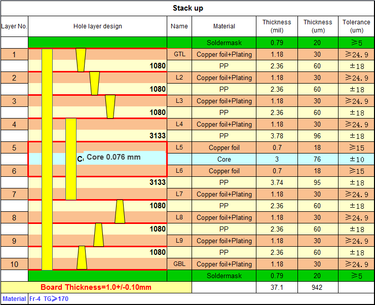
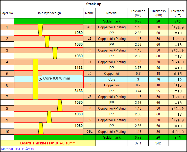
The standard build reaches ten layers in four presses. The first lamination consolidates the rigid core; the next three each add one copper pair and one laser-drilling stage. Table 1 shows the sequence used for the stackup in the hero image of this article, drawn for a 1.0 mm finished thickness.
| Lamination cycle | Layers added | Cumulative layers | Feature completed |
|---|---|---|---|
| Cycle 1 | L4–L7 inner core | 4 | Through-hole and buried-via backbone (mechanical drill) |
| Cycle 2 | L3 + L8 | 6 | Stage-1 laser microvias (L3→L4, L7→L8) |
| Cycle 3 | L2 + L9 | 8 | Stage-2 laser microvias (L2→L3, L8→L9) |
| Cycle 4 | L1 + L10 | 10 | Stage-3 laser microvias (L1→L2, L9→L10) |
Two things are worth noticing. First, the inner four layers behave like a conventional multilayer board: L4–L7 are laminated, mechanically drilled and plated before any microvia work starts, so buried vias connecting L4 to L7 are formed here. Second, each later cycle multiplies the risk of the whole panel — a registration error in cycle 4 scrapes a board that has already absorbed three presses, so late-stage yield dominates the cost of a 10-layer 3-stage HDI stackup.
That is also why fabricators care so much about the details in the stackup table. The next section reads one line by line.
How to Read the Stackup Table: Materials and Tolerances
The hero image in this article is a real factory stackup table for a 1.0 mm board. Table 2 translates its rows into the values that matter for a design review.
| Stackup element | Material | Thickness | Tolerance |
|---|---|---|---|
| Outer and inner copper (plated) | Copper foil + electroplated copper | ≈30 µm (1.18 mil) nominal | ≥24.9 µm finished |
| Prepreg between signal layers | FR-4 prepreg 1080 | ≈60 µm | ±18 µm |
| Prepreg between power pairs | FR-4 prepreg 3133 | ≈96 µm | ±18 µm |
| Inner core | FR-4 core, 0.076 mm, copper-clad both sides | ≈76 µm (3 mil) | ±10 µm |
| Finished board (with soldermask) | Base laminate FR-4, Tg ≥ 170 °C | 1.0 mm nominal | ±0.10 mm |
Three observations. The core is only 0.076 mm of dielectric — thin even by HDI standards — so its ±10 µm tolerance is the tightest number on the sheet and the main constraint on controlled impedance in inner layers. The 1080 and 3133 glass styles are mixed deliberately: thin 1080 sheets give the smooth dielectric the microvia layers need, while thicker 3133 builds up the power-plane separation without adding press count. And the Tg ≥ 170 °C laminate class is what keeps the board dimensionally stable through four press cycles at roughly 180 °C — a lower-Tg FR-4 would drift too much between cycles.
When you compare quotes for a 10-layer 3-stage HDI stackup, check that the fabricator states both thicknesses and tolerances per dielectric, not just a total board thickness. A total-only spec hides which layer absorbs the variation, and that layer is usually the one carrying your fastest signals. Material selection trade-offs across laminate classes are covered in the PCB materials and laminates guide, and the UL recognition of the laminate system itself can be checked against UL Solutions’ yellow card listings.
Via Structures: Blind, Buried and Through in One Board
A standard 10-layer 3-stage HDI stackup mixes all three via families. Stage-1 microvias link L3 to L4 and L7 to L8; stage-2 microvias link L2 to L3 and L8 to L9; stage-3 microvias close the final gap from L1 to L2 and L9 to L10. Inside the core, buried vias connect L4 to L7 without touching either surface, and a smaller number of mechanical through-holes carry power and slow signals from L1 all the way to L10.
The division of labor matters for routing. Fine-pitch BGA fan-out lives in the stage-1 and stage-2 microvias, escape routing tightens as you move outward, and the buried via land inside the core behaves like a conventional multilayer connection. Because each microvia generation must land accurately on the pads of the previous one, the whole structure depends on blind and buried via process control — laser spot size, capture pad size and layer-to-layer alignment move together.
It also matters for test. Through-holes give probing access from both surfaces; a board built without them (see the variants below) must be tested through microvia pads or dedicated test coupons, which is worth flagging to your fabricator before the stackup is frozen.
Simplified 10-Layer 3-Stage HDI Stackup Variants
The standard build is not the only way to reach ten layers with three laser stages. Fabricators keep a small library of variants that trade one constraint for another; the most common are summarized in Table 3, and one of them — the blind-plus-buried build with no through-holes — is shown in the image below.
| Variant | Via structure | Through-holes | Best suited for |
|---|---|---|---|
| Standard (Table 1 build) | Blind + buried + PTH | Yes | Mixed I/O, power entry, back-panel test access |
| Blind-only standard | 3-stage blind vias, no buried pairs | Yes | Cost-sensitive builds with light inner-core routing |
| Blind + buried, no PTH | Blind and buried only | No | Maximum routing density, full-surface BGA fields |
| Simplified A / B | Fewer build-up pairs, 3 laser stages kept | Varies | Fixed-thickness or material-constrained designs |
The no-through-hole variant deserves a note of caution. Removing plated through-holes frees both surfaces for component fields and eliminates the barrel-fatigue concern on thick boards, but every connection now depends on laser microvias and buried vias — so the registration and plating requirements tighten exactly where the board is hardest to rework. Simplified variants go the other way: they keep the three laser stages but reduce build-up pairs, which relieves the lamination budget when the design must stay at 1.0 mm or below.
Choosing between these is a stackup-level decision, not a routing decision. It should be made with the fabricator’s process window in hand — which is precisely what a stackup review at PCB manufacturing services level is for.
Staggered vs Stacked Microvias
Every variant in the previous section is drawn with staggered microvias: each generation is offset horizontally from the one below it, so a stage-2 via lands beside — not exactly on — the stage-1 pad underneath. Staggering is the default because it is cheaper: the laser drills each layer pair independently, plating is straightforward, and small alignment errors do not compound vertically.
Stacked microvias, where each generation sits directly on top of the previous one, shorten the vertical path — which helps escape routing under very fine-pitch BGAs — but they require the lower via to be filled with copper and planarized before the next stage lands on it. Each stacked joint adds a fill-and-planarize cycle, and the alignment requirement tightens because the stacked column must stay within the capture pad at every layer.
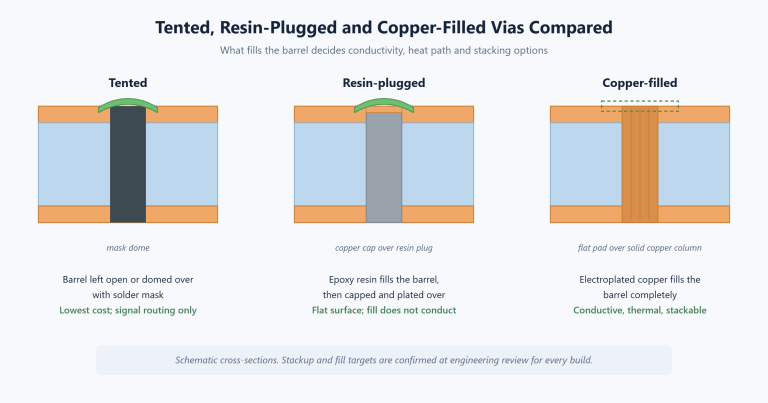
A practical rule: stay staggered unless the BGA pitch genuinely forces stacking, and if you must stack, stack only the outermost stage where fan-out is densest. On a 10-layer 3-stage HDI stackup, converting all three stages to stacked vias is one of the fastest ways to move a design into a different cost class. The copper-filled via process article explains what the fill step involves.
Design Rules That Keep a 3-Stage Build Manufacturable
Third-stage designs fail at the rules level more often than at the equipment level. The parameters below are the ones to check against your fabricator before layout starts, because they interact — shrink one and the others usually tighten too.
- Laser microvia diameter: 0.1 mm is the production-standard minimum; 0.076 mm is achievable but reviewed case by case.
- Microvia aspect ratio: keep it at or below 1:1 (diameter ≥ dielectric thickness) so plating closes the barrel without voids.
- Line and space: 2/2 mil (50 µm) in production; 1.8/1.8 mil for prototype builds under engineering review.
- Build-up thickness per stage: matched to the via diameter so the 1:1 rule holds after lamination squeeze.
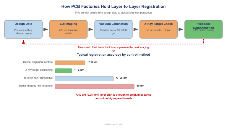
- Layer-to-layer registration: ±25 µm or better across the panel — the controlling spec for stacked via lands.
- Annular ring on microvia capture pads: sized for the actual registration capability, not the nominal drill size.
Registration deserves special emphasis because a 3-stage board amplifies it: each lamination cycle adds a shrinkage contribution, and by cycle 4 the outer layers are landing on features that have already moved three times. How factories measure and compensate that drift is covered step by step in PCB layer-to-layer registration control. For a broader view of where third-stage builds stress a process line, see why advanced HDI is hard to manufacture.
Signal Integrity and Layer Pairing
Ten layers give you room for a disciplined pairing scheme, and a 3-stage build rewards you for using it. A typical arrangement alternates signal and plane pairs — L1 signal over L2 ground, L5–L6 as a power/ground pair in the core, L9 signal over L10 ground — so every high-speed reference has an adjacent return plane two dielectrics away at most.
The microvia layers contribute their own advantage: a 0.1 mm laser via has a stub of a few tenths of a millimetre instead of the several-millimetre stub of a through-hole on a 1.6 mm board. On edges faster than a few gigabits per second, that stub difference is often the real reason a design moves to HDI at all. The price is that inner-layer transitions now pass through two or three via generations, so the return-path discontinuity at each stage transition should be checked in the stackup review, not discovered in the lab.
Impedance tolerance is the contract that holds this together. Production practice is ±10 % for single-ended controlled impedance, ±8 % where the design is sensitive, and ±5 % by case review; state the requirement per layer class in the fab drawing so the stackup table’s dielectric tolerances can be verified against it.
Where 10-Layer 3-Stage HDI Fits
Applications cluster around dense digital processing in a constrained envelope. Network and communications equipment uses the stage count for high-speed memory and SERDES fan-out; computing platforms — blade carriers, AI edge modules, storage controllers — use it to place a large processor plus its power tree on a small board; and industrial control adds the reliability dimension, where the solid copper-filled microvias also improve thermal cycling life.
Automotive electronics is an expanding case: camera and display modules around the cockpit combine dense connectors with tight space, and designs such as an automotive HUD PCB show the direction — when those modules gain processing headroom, they move up the stage ladder. On the computing side, a 14-layer computing PCB illustrates what happens when a 10-layer 3-stage design outgrows its layer budget and the core count takes over.
The common thread is pin density, not raw layer count. If your BGA escapes finish within two routing channels on a 2-stage build, a third stage usually buys cost, not capability. If outer-layer fan-out is exhausted, the 10-layer 3-stage stackup is the natural next rung — and the reference build in this article is a proven starting point for the stackup conversation with your fabricator.
What the Third Stage Adds in Cost and Lead Time
Each additional HDI stage typically raises board cost by roughly 30–100 % relative to the previous stage, because it adds a full process loop: lamination, laser drilling, plating and fill, planarization, and one more round of optical registration checks. On a 10-layer build the through-hole and buried-via backbone is common to all variants, so the stage count is the main lever you control.
Lead time moves the same direction. A 2-stage 8–10 layer prototype typically runs 17–18 working days; a 3-stage build adds at least one lamination and drilling cycle on top, and the exact figure is confirmed at engineering review because it depends on panel utilization and current line loading. Neither number includes design iteration — on third-stage boards the first-pass yield discussion is worth having with your fabricator before the order, since scrap at cycle 4 is the expensive kind.
Two cost levers sit on the design side. Staggered instead of stacked vias removes fill-and-planarize cycles; and a simplified variant (Table 3) that keeps three laser stages but trims build-up pairs can hold performance targets while easing the lamination budget. Both are stackup-level choices — they must be settled before routing locks the layer assignments. The IPC standards for HDI design define the documentation baseline fabricators will quote against.
Frequently Asked Questions
What is a 10-layer 3-stage HDI PCB?
It is a ten-copper-layer board whose interconnect uses three generations of laser-drilled microvias, built sequentially so each new copper pair is laminated, then drilled and plated. Together with mechanical through-holes and buried vias in the core, the three microvia stages give the routing density for fine-pitch processors on a board far smaller than a conventional 10-layer multilayer could be.
How many lamination cycles does a 10-layer 3-stage HDI stackup need?
The standard build takes four: cycle 1 forms the L4–L7 core with its buried vias, then cycles 2, 3 and 4 add the L3/L8, L2/L9 and L1/L10 copper pairs, each followed by a laser-drilling pass. Simplified variants can reduce the press count while keeping the three laser stages, which is one reason they exist.
When is 3-stage HDI worth it instead of 2-stage?
Move to a third stage when outer-layer fan-out is exhausted: BGA escapes that no longer fit in two routing channels, memory interfaces that need shorter via stubs than a 2-stage build allows, or a board area reduction that frees a whole product tier. If a 2-stage 10-layer board still routes cleanly, the third stage typically adds 30–100 % cost for capability you are not using.
What materials are used in a 10-layer 3-stage HDI stackup?
The reference build uses FR-4 laminate with Tg ≥ 170 °C, 1080 and 3133 glass-style prepregs between layers, and a 0.076 mm copper-clad core for the inner four layers. Surface finishes such as ENIG, HASL or OSP are selected per assembly needs. The Tg class matters most: the laminate must stay dimensionally stable through four press cycles near 180 °C.
Should microvias in a 3-stage build be stacked or staggered?
Default to staggered. Each staggered generation is drilled independently, which keeps plating simple and tolerance stack-up forgiving. Stacked microvias need the lower via copper-filled and planarized before the next lands on it, adding a process cycle per joint — so stack only where the BGA pitch forces it, usually at the outermost stage, and keep the rest staggered.
How thin can a 10-layer 3-stage HDI board be?
Around 1.0 mm is the practical reference point for the standard build shown here — a 0.076 mm core plus four build-up stages of 1080/3133 prepreg and ~30 µm copper lands at roughly 0.94 mm before soldermask. Thinner targets are negotiable but they squeeze the 1:1 microvia aspect-ratio rule first, so involve the fabricator’s stackup review before committing.
How do I get a 10-layer 3-stage HDI stackup reviewed?
Submit your Gerber and drill data with the target layer count, thickness and impedance classes; a stackup review returns a proposed lamination sequence, via structure and tolerance table that matches the factory’s process window. Season PCB runs this review in-house across 1/2/3-stage and Any-layer HDI builds, and flags registration or aspect-ratio conflicts before they reach production.
Get Your 10-Layer 3-Stage HDI Stackup Reviewed
Season PCB (998 PCB Group, manufacturing since 2006 across Shenzhen, Jiangxi and Anhui) builds 1/2/3-stage and Any-layer HDI from 2 to 30 layers, with 0.1 mm laser microvias, 2/2 mil line and space, and ±25 µm registration control on third-stage builds. Submit your Gerber package for a stackup review and you will get a proposed lamination sequence, via structure and tolerance table based on the current process window — before you commit routing to a stackup that may not be buildable as drawn. You can also compare a proven 10-layer 2-stage HDI prototype or our 10-layer HDI industrial control PCB as references for the step up to three stages.