Book Appointment Now

A fabricator-side look at advanced HDI PCB production: microvia limits, registration error, copper fill, inspection blind spots and the real yield picture.
Why Advanced HDI PCB Manufacturing Is Hard: Microvias, Yield and Cost
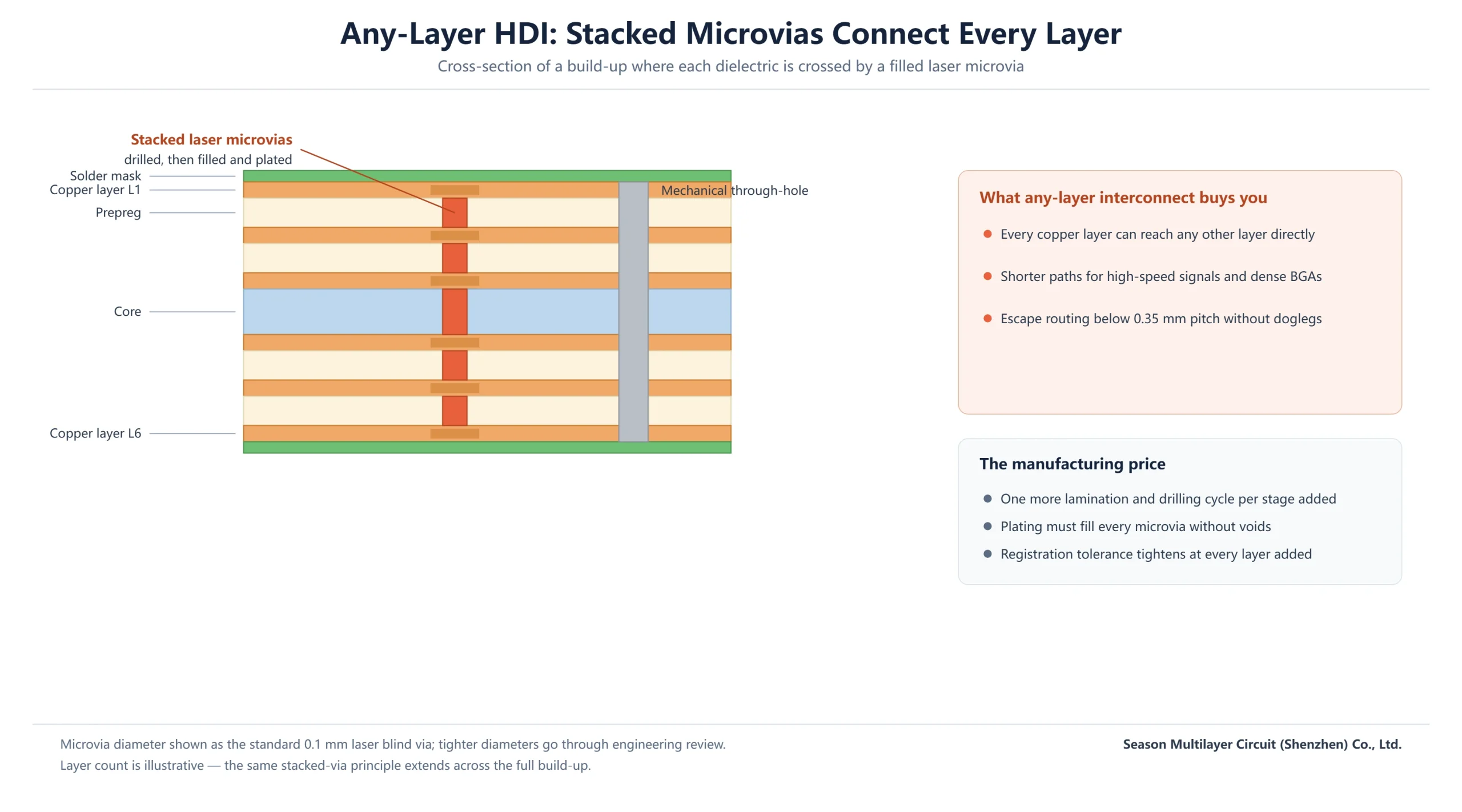
An advanced HDI PCB — 3-Stage and any-layer builds with stacked microvias, sub-40 µm lines and dielectrics thinner than a human hair — is where board fabrication runs closest to its physical limits. It is also where yields quietly drop and quotes climb: industry data puts average yield 15–25% below conventional PCB production, with cost 40–60% higher, and the gap is not price-gouging. It is the measurable price of tighter physics at every step.
This guide explains, stage by stage, where that difficulty actually comes from: microvia drilling at the edge of what lasers can do, layer registration fighting thermal expansion, plating chemistry fighting voids, imaging fighting side etch, and inspection fighting its own resolution limit. By the end you will know which design choices drive cost on an advanced build, which tolerances are worth paying for, and what a capable fabricator does differently.
Table of Contents
- What Counts as Advanced HDI?
- Laser Microvia Drilling at the Physical Limit
- Layer Registration: Error Compounds Every Stage
- Material Bottlenecks Behind Advanced HDI PCB Builds
- Copper Fill: Winning the War on Voids
- Fine-Line Imaging and Etching Control
- Inspection Blind Spots in Advanced HDI PCB
- Yield and Cost: What Buyers Should Expect
- How Capable Fabricators Close the Gap
- FAQ
- Have Your Advanced HDI Stackup Reviewed Before You Quote
What Counts as Advanced HDI?
HDI progresses in stages. A 1-Stage build adds one layer of laser-drilled microvias on each side; a 2-Stage build stacks a second set, a 3-Stage build a third, and any-layer HDI lets every copper layer connect directly to its neighbours without relying on through-holes. Each additional stage means another lamination cycle, another drilling pass and another round of registration — which is why difficulty scales geometrically, not linearly, with stage count. Our HDI PCB technology guide covers the stage definitions in detail.
Advanced territory starts where the numbers stop being forgiving. Line width and spacing that mainstream HDI handles at 75–100 µm drops to around 30 µm. Microvias shrink from 0.15 mm to 0.1 mm and below, with leading products pushing under 0.075 mm. Dielectric layers thin from 0.1 mm toward 0.03 mm. Each of those moves pushes a different process step toward its physical limit.
| Parameter | Mainstream HDI (1-Stage / 2-Stage) | Advanced HDI (3-Stage / Any-layer) |
|---|---|---|
| Minimum line width / spacing | 75–100 µm | Down to ~30 µm |
| Microvia diameter | 0.15 mm | 0.1 mm and below (0.075 mm at the frontier) |
| Stacked via aspect ratio | Moderate | Commonly above 8:1, up to 12:1 |
| Dielectric thickness between layers | ~0.1 mm | 0.06 mm and below (0.03 mm at the frontier) |
| Layer-to-layer registration | ±50 µm | ±25 µm, ±15 µm at the leading edge |
| Lamination cycles | 2–3 | 4 or more |
Laser Microvia Drilling at the Physical Limit
Microvia formation is the step that defines HDI, and it is unforgiving below 0.1 mm. CO2 laser systems — the industry workhorse — become extremely sensitive to beam focus, pulse energy control and heat input at that scale. As diameter drops from 0.15 mm toward 0.08 mm, hole wall roughness climbs by around 50%, and rough walls poison the plating step that follows: electrolyte flows less freely inside the hole, copper deposits unevenly, and voids form. Measured across the industry, void rates that sit within 3% for microvias of 0.1 mm and above can rise to 8–10% once diameter reaches 0.075 mm.
Aspect ratio compounds the problem. Stacked via structures commonly exceed 8:1 and can reach 12:1, and at those ratios electrolyte circulation inside the hole nearly stalls — copper thickness at the bottom of the via can fall to 30–40% of the top, the classic dog-bone profile. That thinning shows up later as impedance discontinuity and a reliability liability on high-speed nets. Fabricators who build advanced HDI PCB products seriously run UV and picosecond laser systems alongside CO2: picosecond pulses finish machining before heat spreads, cutting the heat-affected zone from 15–20 µm to under 5 µm and improving wall roughness by more than 40% — at the price of equipment cost two to three times higher and throughput down 20–30%.
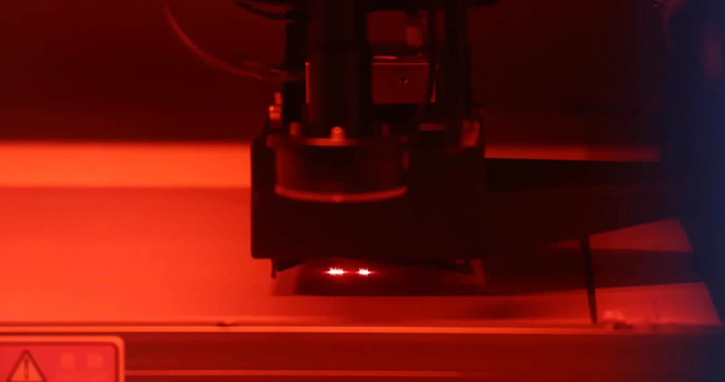
The practical takeaway for a buyer: microvia diameter is not a free parameter. Every 10 µm below 0.1 mm buys fanout density but moves the build onto scarcer equipment, slower cycles and a thinner yield margin. On our line, 0.1 mm laser blind vias are standard production; diameters approaching 0.076 mm are achievable on engineering review, per build.
Layer Registration: Error Compounds Every Stage
Registration tolerance has tightened from ±50 µm a generation ago to ±25 µm in volume production and ±15 µm at the leading edge — while the materials themselves fight back. FR-4 expands 14–16 ppm/°C in plane; copper, about 17. On an 18 × 24 inch panel heated from room temperature to a 180 °C lamination window, that mismatch alone produces more than 200 µm of dimensional change — an order of magnitude larger than the tolerance the stack must hold.
Fabricators manage it with high-accuracy alignment systems (infrared and X-ray-based, holding ±25 µm), per-material shrink compensation learned from measured process data, and post-cycle adjustments rather than one fixed recipe. In any-layer constructions the problem bites hardest, because every layer pairs directly with every other — there is no design trick that hides a misregistered via pad. Industry experience puts scrap from registration deviation at around 7% on 12-layer any-layer builds, making it one of the top two yield killers in advanced HDI PCB production.
Material Bottlenecks Behind Advanced HDI PCB Builds
The materials an advanced build wants are the materials that are hardest to process. Low-loss resin systems and PTFE-class laminates deliver excellent Df at high frequency but warp in thin constructions and expand differently from copper, worsening the registration problem above. Thin dielectrics — 0.06 mm and below, with thickness held to ±5% where standard laminate tolerance runs ±10% — cost multiples of ordinary FR-4. The table below summarises the trade-offs every advanced stackup negotiates.
| Material requirement | Why the build needs it | Engineering trade-off |
|---|---|---|
| Low-Df laminate at high frequency | Signal integrity on multi-gigahertz nets | Harder to process; warp and CTE mismatch stress registration |
| Thin, uniform dielectric (±5%) | Fine-pitch breakout and short via stubs | Specialty materials cost multiples of standard FR-4 |
| Low-profile copper foil (Rz below 2 µm) | Conductor loss at high frequency — insertion loss improves 15–20% at 10 GHz versus standard foil | Smoother foil bonds less strongly: peel strength falls from ~1.2 to ~0.8 N/mm |
| Low-CTE resin system | Registration survives reflow and thermal cycling | Newer resin chemistry carries a cost premium |
| Dimensional stability in plane | Layer alignment across lamination cycles | Constrains panel size and construction choices |
The copper-foil trade-off deserves special attention, because it looks like a free win and is not. Conductor loss concentrates at the conductor surface at high frequency, so ultra-low-profile foils genuinely buy insertion-loss margin. But adhesion strength drops as roughness falls, and temperature cycling then works on a weaker bond. Leading fabricators qualify foil systems by peel strength after thermal stress, not by roughness numbers alone — a question worth asking any prospective supplier.
Copper Fill: Winning the War on Voids
A stacked microvia is only as good as its fill. Every microvia must be filled solidly with copper — a residual void becomes a stress concentration, a thermal-cycle failure seed and, on RF paths, an impedance surprise. Fill quality is governed by electroplating chemistry and by a narrow operating window: on 0.08 mm microvias, the working current density sits around 1.8–2.2 A/dm². Below roughly 1.5, plating takes so long that the via mouth closes over first, trapping a void inside; above roughly 2.5, the mouth deposits too fast and the same void forms from the other direction.
Holding that window across a full panel — through bath chemistry drift, temperature swings and via density variation — is a genuine process-control achievement. Pulse plating changed the economics: by shaping the current waveform, frequency and duty cycle, fabricators improve copper distribution inside the via, and published fabricator results show fill void rates dropping from around 8% to below 2% while throughput rises roughly 15%. It is one of the few advanced-HDI investments that improves both quality and cost simultaneously.
Fine-Line Imaging and Etching Control
At 30 µm line width, every µm of error is proportionally huge. Liquid photoresists stop resolving somewhere below that class, so fine-line work moves to dry film — which has limits of its own. Imaging splits accordingly: conventional contact exposure risks dust and damage between mask and panel, while laser direct imaging avoids the mask entirely and holds geometry tight, at lower throughput and higher cost per panel. Design data quality matters more here than anywhere else in the process, so clean Gerber data directly reduces imaging defects.
Etching is the quieter problem. Horizontal etch lines run 15–20% side etch, which on a 30 µm line eats 4.5–6 µm per side — a third of the line gone. Vertical etch equipment holds side etch under 5%, but the equipment costs more than 50% extra and consumes more chemistry. The etch factor (copper thickness divided by horizontal undercut) becomes the specification that separates suppliers who can hold 30 µm lines in production from those who hold them on a good day. The broader context sits in the IPC standards governing build-up and microvia design.
Inspection Blind Spots in Advanced HDI PCB
Detection is its own engineering problem, because the defects that matter are now smaller than the tools that hunt them. Automatic X-ray inspection resolves 1–2 µm at best, but critical voids in sub-0.08 mm microvias measure under 1 µm. Fabricator statistics put missed detection of bubbles in sub-0.05 mm vias as high as 15% — defects that surface later, in the field, as failures nobody screened out.
Electrical test has a parallel gap. Flying-probe tips measure 50–100 µm across, while advanced test point pitch has fallen below 150 µm, producing false-short misjudgement rates that can reach 20% on sub-30 µm geometries — good boards scrapped, or worse, marginal ones passed. In-line machine vision fares no better at production speed: capture rates for micro defects fall below 70% at panel speeds of 1.5–2 m/min. Machine-learning defect classification is closing the gap — deep-learning models trained on X-ray image sets have lifted detection accuracy on sub-0.05 mm voids from 85% to 96% in published deployments — but no honest fabricator will claim the blind spots are gone.
Yield and Cost: What Buyers Should Expect
Put the physics together and the commercial picture follows directly. Yield on advanced HDI PCB builds runs roughly 75–85% where conventional multilayer production sits near or above 95%, and cost lands 40–60% higher, driven by slower equipment, specialty materials, more lamination cycles and the scrap that tighter tolerances imply. As a rule of thumb from stage-count economics, each additional HDI stage typically adds 30–100% to build cost; the premium buys geometry that no other construction can deliver.
| Cost and yield driver | Effect on the build |
|---|---|
| Each additional HDI stage | One more lamination cycle, drill pass and registration round; cost typically +30–100% per stage |
| Microvia density | More drilling and plating time per panel; void-rate risk rises below 0.1 mm |
| Thinner dielectric and specialty laminates | Material cost multiples of FR-4; tighter incoming inspection |
| Registration spec at ±25 µm or tighter | Scrap risk concentrates here — roughly 7% on 12-layer any-layer builds |
| Inspection depth (AXI, flying probe, coupon density) | Test cost up, but escaped defects cost more than screening does |
Lead times follow the same logic: an 8–10 layer 2-Stage HDI prototype typically runs 17–18 working days on our floor, and advanced 3-Stage or any-layer builds take longer, with the honest number confirmed at engineering review once the stackup is known. Quotes vary more at this end of the market than anywhere else in PCB — the fabricator’s equipment base and yield history, not any price list, sets the number.
How Capable Fabricators Close the Gap
The difficulty is real but not static, and the improvements are specific. On materials: low-CTE resin systems have cut in-plane expansion from 14–16 to 8–10 ppm/°C, shrinking the mismatch with copper by half and lifting registration capability from ±25 µm toward ±18 µm on 12-layer builds. Ultra-low and very-low-profile foils now hold Rz below 1 µm while keeping peel strength at acceptable levels through improved surface treatment.
On process: adaptive laser-energy control adjusts drilling parameters in real time per hole, improving wall roughness around 30% and hole position accuracy around 25%; pulse plating holds the fill window and drives void rates toward 2%. On inspection, ML-based X-ray classification is closing the detection gap noted above. None of these are marketing; each maps to a defect mechanism described earlier in this article, and a serious supplier will show you the data behind any of them.
Where we sit in that picture: 998 PCB Group has produced HDI since 2006 across three plants — Shenzhen, Jiangxi and Anhui — with 2–30 layer capability, 3,000,000 m² annual capacity, 0.1 mm laser blind vias as standard production (0.076 mm achievable per engineering review), 2/2 mil line and space (1.8/1.8 mil on samples), blind via aspect ratio at 1:1, and 4+N+4 constructions with resin plugging and electroplated fill. Practical examples include our 10-layer 2-Stage HDI prototype PCB and 14-layer 2-Stage HDI prototype builds. For stage definitions and stackup selection logic, see the companion article on 1-Stage vs 2-Stage vs 3-Stage HDI.
Frequently Asked Questions
What is an advanced HDI PCB?
An advanced HDI PCB is a high-density interconnect board at the demanding end of the technology: 3-Stage or any-layer constructions with stacked laser microvias, line width around 30 µm, microvias of 0.1 mm and below, and dielectric layers thinner than 0.06 mm. Smartphones, 5G infrastructure, radar modules and high-speed computing all sit in this class.
How many HDI stages do advanced builds use?
HDI progresses by stage: 1-Stage, 2-Stage, 3-Stage and any-layer. Advanced builds generally mean 3-Stage and any-layer, where microvias stack across multiple dielectric layers and every copper layer can connect directly to its neighbours. Each additional stage adds a lamination cycle and a drilling pass, which is why cost rises 30–100% per stage as a rule of thumb.
Why is yield lower on advanced HDI PCB production?
Three mechanisms dominate: microvia void rates rise sharply below 0.1 mm diameter, registration error from thermal expansion mismatch causes roughly 7% scrap on 12-layer any-layer builds, and sub-30 µm lines are exposed to side-etch error that mainstream geometries shrug off. Industry averages run 15–25% below conventional PCB yield, typically 75–85% on advanced builds.
What is the smallest microvia size a fabricator can build reliably?
It depends on the fabricator’s laser base. 0.1 mm laser blind vias are standard production on capable lines; diameters approaching 0.076 mm are achievable per engineering review, with the frontier of the industry below 0.075 mm. Below 0.1 mm, expect the fabricator to review aspect ratio, plating fill and inspection coverage before committing — that review is a good sign, not a delay tactic.
How does lead time differ for advanced HDI prototypes?
Expect longer than conventional multilayer prototypes: an 8–10 layer 2-Stage HDI prototype typically runs 17–18 working days, and 3-Stage or any-layer builds add lamination and drilling cycles on top. The reliable number comes from an engineering review of your actual stackup — quotes given without one tend to be optimistic.
How can I reduce cost on an advanced HDI design?
Stage count is the biggest lever — dropping one stage where a staggered via would work instead of a stacked one typically saves 30–100% of that stage’s cost. Then relax tolerances that are not load-bearing: microvia diameter just above 0.1 mm, registration at ±25 µm rather than tighter where the design allows, and dielectric thickness no thinner than the breakout actually requires. Panel utilisation and process-friendly laminates close the remaining gap.
What data should I send for an advanced HDI quote?
Gerber and drill data, the proposed stackup with dielectric thicknesses, target impedances with tolerances, expected maximum microvia counts per layer, and the application environment. Include any known cost drivers such as stacked versus staggered via preferences. A fabricator running engineering review on this package will quote a buildable number instead of a best case.
Have Your Advanced HDI Stackup Reviewed Before You Quote
Send your Gerber package, stackup proposal and target impedances through our PCB manufacturing services page. The engineering review returns a manufacturability assessment — stage count, microvia sizes, fill strategy and registration plan — with a firm quotation based on the way we actually build, not the way a price list wishes we did. If the design sits closer to the limit than it needs to, the review will say so and propose the cheaper construction that still meets your electrical targets.