Book Appointment Now

6-layer optical module PCBs for 100G/400G transceivers — ±5% impedance control, RO4350B/FR-4 hybrid stackups, 48–72h prototypes. Request a quote.
6-Layer Optical Module PCB Manufacturing
Engineered for ultra-high-speed data transmission in 10G/25G/100G/400G optical transceivers. Our 6-layer optical module PCB features strict ±5% impedance control, low-loss dielectric materials, and ENIG + hard gold finger plating — built to deliver uncompromising signal integrity in the most compact SFP/QSFP/OSFP form factors.
Every optical module PCB is built on a proven 6-layer stackup with dedicated high-speed signal layers, solid reference planes, and POFV resin-plugged vias — validated by Polar CITS800s pre-production simulation and TDR impedance testing. From 48–72 hour expedited prototypes to 100,000+ piece volume production, we support mixed-dielectric stackups (High-Tg FR4, Megtron 6/7, Rogers) for data center, telecom, and 5G applications. Explore our fast PCB manufacturing services or upload your Gerber files for a free DFM review.
✓ 5-7 Day Quick-Turn
48–72h expedited service available
✓ 1-100,000+ Pieces
From NPI prototypes to mass production
✓ Free DFM Check
Engineering feedback with every quote
✓ 24h Quotation
Fast, transparent pricing
✓ Hybrids & Mixed Dielectrics + POFV
Rogers / Megtron / High-Tg FR4 stackups
✓ ±10% Impedance Control
±5% precision available · TDR verified
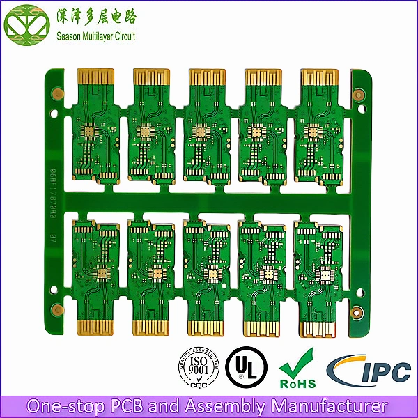
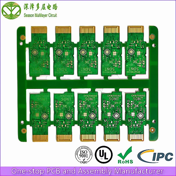
6
Layer Count
4/4 mil
Min. Trace / Space
0.20 mm
Min. Via Diameter
Tg 180
Glass Transition Temp
2 µ”+30 µ”
ENIG + Hard Gold Finger
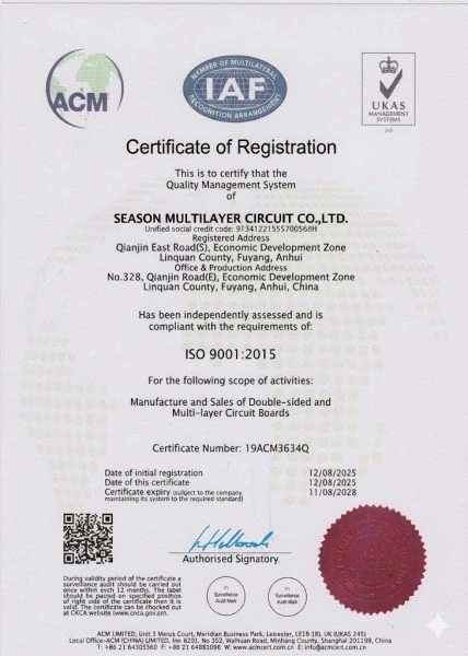
ISO 9001:2015
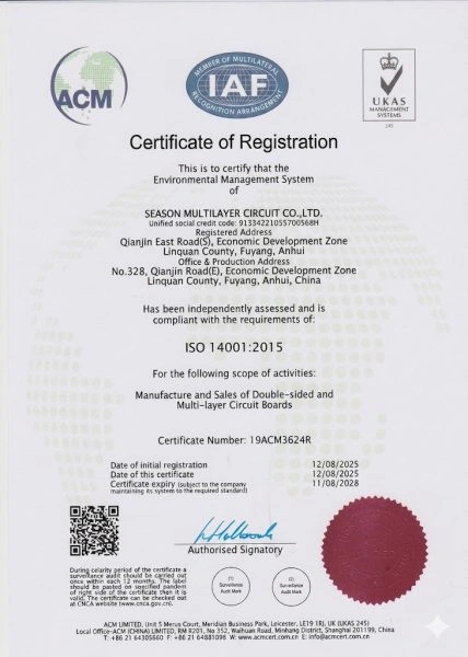
ISO 14001
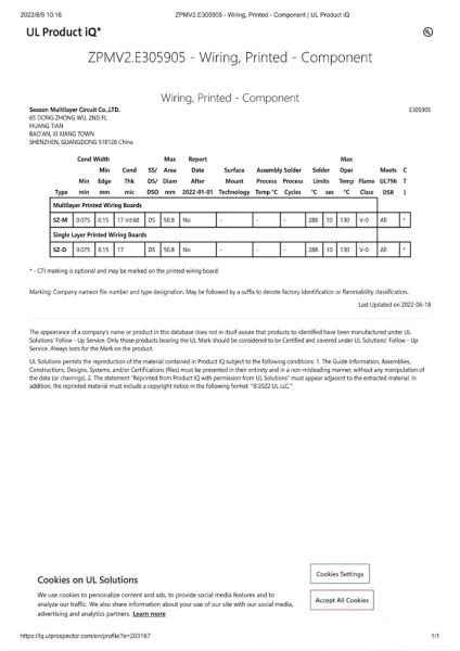
UL (E305905)
IPC Class 2 / Class 3
IATF 16949
RoHS
Optical Module PCB Stackup Design for 100G/400G Transceivers
A well-designed stackup is crucial for electromagnetic compatibility (EMC) and power integrity (PI). Our recommended high-speed 6-layer configuration is a hybrid construction: two Rogers RO4350B cores (0.1 mm) bonded to an FR-4 IT180A core (Tg 180°C) with 3313/106 prepreg, holding a 1.0 ± 0.1 mm finished thickness while keeping low-loss dielectric adjacent to every high-speed differential pair:
- Layer 1 (Top) – Signal (Component): High-speed differential pairs and component placement on a Rogers RO4350B core. Finished copper 1.57 mil (≈1 oz, foil + plating).
- Layer 2 – Ground (GND): Reference plane for Layer 1 and EMI shielding. 0.5 oz copper (0.7 mil foil).
- Layer 3 – Inner-Layer Signal / Routing: Low-speed signals and control lines. 0.5 oz copper on the FR-4 IT180A core.
- Layer 4 – Power (PWR) / GND: Power distribution network (PDN) in a copper-balanced construction. 0.5 oz copper.
- Layer 5 – Ground (GND): Reference plane for Layer 6. 0.5 oz copper.
- Layer 6 (Bottom) – Signal (Gold Finger): Edge-connector routing (gold fingers) and auxiliary components. Finished copper 1.57 mil (≈1 oz, foil + plating).
The dielectric layers pair two Rogers RO4350B cores (0.1 mm) with an FR-4 IT180A core (0.33 mm) bonded by 3313/106 prepreg — core and prepreg thicknesses are base-laminate values (copper excluded), as marked on the stackup drawing. This hybrid stackup keeps low-loss RO4350B adjacent to every high-speed pair while total finished thickness holds at 1.0 ± 0.1 mm.
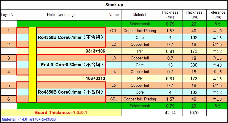
Stackup Optimization Service: If your original design does not meet strict impedance requirements, our engineering team will optimize the stackup for you — adjusting dielectric thicknesses, copper weights, and material selections to achieve your target impedance values. We provide pre-production stackup simulation reports using Polar CITS800s instrumentation to verify performance before manufacturing begins.

Technical Specifications & Manufacturing Capabilities
The table below details the specifications for our standard 6-layer optical module PCB, along with our full advanced manufacturing capabilities. Custom configurations are available — contact our engineering team to discuss your specific requirements.
| Parameter | Specification | Advanced Capabilities |
|---|---|---|
| Layer Count | 6 Layer | 2–32 layers (mass); 2–64 layers (sample) |
| Base Material | FR-4 (IT180A, Tg 180°C) | SY, NY, TUC, ZY, EMC, KB, ITEQ, Rogers, Megtron, Nelco, Isola |
| Board Thickness | 1.0mm | 0.2–6.4mm (mass); 0.15–20mm (sample) |
| Panel Size | 83.2 × 68.4mm / 10-up | 800 × 600mm (mass); 1050 × 610mm (sample) |
| Copper Thickness | Outer: 1 oz Inner: 1 oz | Outer: 1/3–12 oz Inner: 1/4–12 oz |
| Min Drill Size | 0.2mm | 0.15mm (mass); 0.127mm (sample) |
| Min Trace Width/Spacing | 4/4 mil | 2.5/2.5 mil (1 oz) 2/2 mil (0.5 oz) |
| Min BGA Pad | N/A | 0.15mm |
| Surface Finish | ENIG 2 µ”+Electric Hard Gold 30 µ” | OSP, ENIG, HASL, Electric Hard Gold, ENIG+OSP, ENEPIG, Immersion Silver & Tin |
| Specialized Processes | POFV | Resin Plugged Vias, Copper Paste Via Filling, Copper Plating Via Filling |
| Solder Mask Color | Green | Green, Blue, Black, White, Yellow, Red, Purple, Matte Green, Matte Blue, Matte Black |
| Impedance Control | ±10% (50/85/100Ω) | ±5% (strict tolerance) |
| Min Routing Tolerance | ±0.15mm | ±0.075mm |
| Quality Standard | IPC-6012 Class 2, RoHS | IPC-6012 Class 3, UL, RoHS, IATF 16949, GJB |
| PCB Type | Multilayer | HDI, Multilayer, Rigid-Flex, High Frequency, High Speed, Hybrids & Mixed Dielectrics |
Why 6-Layer Optical Module PCBs for High-Speed Transceivers
Optical transceiver modules are the backbone of modern high-speed data center interconnects, telecommunications infrastructure, and 5G wireless networks. As data rates scale from 10G to 400G and beyond, the printed circuit board (PCB) inside these modules must handle increasingly demanding signal integrity, thermal management, and mechanical reliability requirements — all within an extremely compact footprint.
Our 6-layer PCB for optical modules is purpose-built for these challenges. With a carefully optimized layer stackup that isolates high-speed differential pairs, dedicated ground and power planes for superior EMI performance, and advanced low-loss dielectric materials, this PCB ensures clean signal transmission at data rates up to 400Gbps. Whether you’re designing SFP+, SFP28, QSFP28, CFP4, or OSFP modules, our manufacturing capabilities deliver the precision and reliability your optical communication systems demand.
Backed by over a decade of experience in high-speed PCB manufacturing, Season PCB provides end-to-end support — from DFM (Design for Manufacturing) consultation and stackup optimization to volume production and rigorous quality testing. Every board is manufactured in our ISO 9001:2015 certified facility and 100% electrically tested before shipment.
Key Highlights at a Glance
Optical Module PCB Core Features & Advantages
Optical module PCBs operate at the intersection of high-frequency signal integrity, thermal stress, and mechanical precision. Our 6-layer PCB solution addresses each of these dimensions with engineering-grade rigor:
Ultra-High-Speed Signal Integrity
Designed for 25G/lane and 50G/lane differential pairs with precise trace geometry control. Low-loss dielectrics (Rogers RO4000, Megtron 6/7) minimize insertion loss and skin-effect attenuation, ensuring clean eye diagrams at 100G/400G data rates — where channel harmonics extend well into the tens of GHz.
Precision Impedance Control
±10% controlled impedance as standard, with ±5% precision available for mission-critical applications. Polar CITS800s pre-layout simulation ensures stackup accuracy before production, and TDR testing validates every batch.
Hard Gold Finger Plating
Edge connectors receive hard gold plating (≥30 µ”) over nickel for exceptional wear resistance — rated for 500+ insertion cycles. The rest of the board uses ENIG for superior solderability on fine-pitch BGA and QFN components.
Advanced Thermal Management
Integrated thermal vias beneath laser drivers (EML/DFB) and ASICs efficiently conduct heat away from hot spots. Heavy copper options (up to 12 oz) available for high-power designs, preventing thermal throttling in dense 400G QSFP-DD modules.
Compact HDI Routing
For ultra-compact SFP and QSFP form factors, we offer HDI build-ups with 3 mil laser-drilled microvias and 2/2 mil fine-line routing. POFV (Plated Over Filled Via) technology maximizes routing density without sacrificing reliability, and via-in-pad microvias free up escape channels under fine-pitch BGAs.
EMI Shielding & EMC Compliance
The dedicated ground planes in our 6-layer stackup provide continuous return paths for high-speed signals, minimizing electromagnetic emissions and crosstalk. This ensures compliance with FCC, CE, and CISPR standards for optical communication equipment.
Comprehensive Material Options
From cost-effective High-Tg FR4 (Tg≥170°C) for 10G/25G modules to ultra-low-loss Rogers and Megtron 7 for 400G+ applications — we match the dielectric to your data rate, loss budget, and cost targets. CAF-resistant and halogen-free laminate systems are available for high-reliability and environmentally constrained designs.
100% Quality Assurance
Every board undergoes AOI, X-ray inspection, microsection analysis, flying probe / universal electrical testing, and TDR impedance verification. Manufactured to IPC-6012 Class 2 as standard with IPC-2221 design support; IPC-6012 Class 3 available for mission-critical deployments.
Scalable Production Volume
From quick-turn prototypes (48–72 hours) to volume production with consistent quality — our facility supports panel sizes up to 800 × 600mm for mass production and 1050 × 610mm for samples, ensuring cost efficiency at any scale.
Optical Module PCB Design Challenges and Our Solutions
Optical modules demand ultra-high reliability in extremely confined spaces. As data rates climb from 25G to 100G to 400G per lane, traditional PCB designs face critical bottlenecks in signal integrity, thermal management, and mechanical precision. Each challenge below is paired with the manufacturing countermeasure we apply to your 6-layer PCB:
Signal Degradation at High Data Rates
At 25G/lane and above, dielectric loss (Df) and conductor skin effect attenuate the signal — insertion and return loss roll off with frequency until eye diagrams close. Our countermeasure: ultra-low-loss laminates (Rogers RO4000 series, Megtron 6/7, Nelco N4000-13, Df as low as 0.002), precision trace geometry, and back-drilling of via stubs to preserve channel bandwidth — see Ultra-High-Speed Signal Integrity above.
Impedance Mismatch & Reflections
Even small impedance deviations cause reflections that corrupt high-speed data. Our countermeasure: ±10% impedance control as standard (±5% on request) for 90Ω/100Ω differential and 50Ω/85Ω single-ended pairs, verified by Polar pre-layout simulation and batch TDR measurement — see Precision Impedance Control above.
Thermal Dissipation in Compact Spaces
Laser drivers (EML/DFB) and transimpedance amplifiers generate significant heat in a tiny footprint, and performance degrades as temperatures climb. Our countermeasure: thermal via arrays directly under hot components, heavy copper up to 12 oz for power stages, and copper-balanced stackups that spread heat across the board — see Advanced Thermal Management above.
Routing Density in Miniature Form Factors
SFP and QSFP modules have extremely limited board area, requiring dense routing around BGAs and connectors. Our countermeasure: HDI build-ups with 3 mil laser-drilled microvias, 2/2 mil fine-line routing, POFV, and back-drilled through-hole stubs — see Compact HDI Routing above.
Gold Finger Wear & Reliability
Optical modules are frequently inserted and removed, subjecting edge connectors to mechanical wear. Our countermeasure: hard gold plating (≥30 µ” over nickel) rated for 500+ insertion cycles, with beveled edge chamfering to reduce insertion force — see Hard Gold Finger Plating above.
EMI Emissions & EMC Compliance
High-speed differential pairs radiate electromagnetic energy that can interfere with adjacent modules and fail regulatory tests. Our countermeasure: dual ground planes (L2 and L5) forming a Faraday-cage return path, contained within FCC Part 15, CE EN 55032, and CISPR 32 limits — see EMI Shielding & EMC Compliance above.
Material Selection Guide for Optical Module PCBs
Choosing the right dielectric material is critical for balancing signal performance, thermal reliability, and cost. Above roughly 10 GHz, dielectric loss takes over most of the channel budget, so Dk, Df and their stability over frequency decide how far a link can run before the eye closes. The table below maps data rate to the material class we recommend, from legacy NRZ designs up to 400G/800G PAM4:
| Data Rate | Recommended Material | Dk (Dielectric Constant) | Df (Loss Tangent) | Typical Application |
|---|---|---|---|---|
| 1G – 10G | High-Tg FR4 (IT180A, S1000-2M Tg≥170°C) | 4.2 – 4.6 | 0.010 – 0.015 | SFP, SFP+ (10G Ethernet, Fibre Channel) |
| 10G – 25G | Mid-Loss FR4 (TUC, ITEQ, EMC, SY) | 3.8 – 4.2 | 0.005 – 0.008 | SFP28 (25G Ethernet, 5G fronthaul) |
| 25G – 100G | Low-Loss (Megtron 6, Nelco N4000-13, S7439C) | 3.4 – 3.7 | 0.002 – 0.004 | QSFP28 (100G data center interconnect) |
| 100G – 400G+ | Ultra-Low-Loss (Megtron 7, Rogers RO4000, Synamic8GN) | 3.0 – 3.5 | 0.001 – 0.002 | QSFP-DD, OSFP (400G/800G hyperscale) |
Hybrid Stackup Option: For cost-sensitive designs, we can build hybrid stackups that combine low-loss material on critical high-speed signal layers with standard FR4 on power and ground layers — achieving near-equivalent signal performance at a significantly lower material cost. This is especially valuable for volume production of 25G/100G optical modules where bill-of-materials (BOM) cost is a key competitive factor. Every laminate we specify is a UL 94 V-0 rated flame-retardant system.
Supported Optical Module Form Factors
Our 6-layer PCBs are engineered to fit the mechanical and electrical specifications of all major optical transceiver industry standards. We have extensive manufacturing experience across the full range of form factors used in modern optical communication systems:
SFP+ (10G)
Small Form-factor Pluggable for 10G Ethernet, Fibre Channel, and SONET/SDH applications. Board dimensions typically 56.5 × 8.5 mm. Our SFP+ PCBs run 10.3125 Gbps per lane with ±10% impedance control as standard, on both cost-effective High-Tg FR4 and low-loss laminates — and high-volume panelization on 83.2 × 68.4 mm / 10-up panels keeps unit cost low across 1G–10G module families.
SFP28 (25G)
25G Ethernet and 5G wireless fronthaul (CPRI/eCPRI). Same mechanical footprint as SFP+ with enhanced signal integrity requirements. At 25.78125 Gbps per lane we control impedance to ±10% (±5% on request), specify mid-loss laminates (TUC, ITEQ, EMC), and back-drill via stubs at connector breakouts to protect channel margin — with −40°C to +85°C material options for outdoor base station deployments.
SFP56 (50G)
50G Ethernet for next-generation campus and data center interconnects. PAM4 signaling and tighter impedance control define this tier: at 53.125 GBd PAM4 we recommend low-loss materials (Megtron 6 class, Df ≤ 0.004), 2/2 mil routing, and laser-drilled microvias to escape the 50G DSP footprint inside the SFP56 outline.
QSFP+ (40G)
Quad Small Form-factor Pluggable for 40G Ethernet and InfiniBand. 4×10G lanes with an integrated heat sink interface. Four parallel differential pairs make length matching and skew control critical — we hold pair-to-pair skew tight across the breakout region and verify every lane with TDR on production coupons before shipment.
QSFP28 (100G)
100G Ethernet data center interconnects. 4×25G lanes demanding low-loss materials and precise differential pair routing. We build QSFP28 PCBs on Megtron 6 / Nelco class laminates with Df ≤ 0.004, controlled 100Ω differential impedance, and copper-balanced stackups for reliable lamination at volume.
QSFP56 (200G)
Double-density QSFP for 200G Ethernet. 4×50G PAM4 lanes in the QSFP56 outline push channel frequencies higher, so material selection and via stub management dominate the link budget. We combine low-loss laminates, back-drilled escape vias, and ±5% impedance control on request to hold insertion loss within budget.
QSFP-DD (400G/800G)
Double-density QSFP for 400G/800G hyperscale data centers. 8×50G or 8×100G lanes — the most demanding PCB design challenge in volume optics. Ultra-low-loss materials (Megtron 7, Rogers RO4000), HDI microvias, POFV, and strict skew control keep eight parallel channels within spec across the full operating temperature range.
OSFP (400G/800G)
Octal Small Form-factor Pluggable for next-gen 400G/800G networks. Larger form factor with integrated thermal management features. The extra board area accommodates heavier copper (up to 12 oz) power layers and thermal via arrays under the DSP, while HDI routing handles eight high-speed lanes in a compact keep-out zone.
CFP / CFP2 / CFP4
Designed for long-haul coherent optical transport networks (100G–400G). Larger board area supporting complex coherent DSP ASICs. Multi-row BGA breakouts, back-drilled fanouts, and low-CTE hybrid stackups maintain layer alignment and channel performance in DWDM and submarine-line applications.
Active Optical Cables (AOC)
High-density PCB layouts for short-range, high-speed active cabling solutions used in server-to-server and rack-to-rack connections. AOC boards integrate driver and CDR ICs close to the connector, so we focus on microvia-in-pad, POFV, and impedance continuity through tight BGA escape routing.
Board-Mounted Optics (BO)
Board-mounted optical engines for embedded optical interconnects — the most compact form factor, requiring full HDI construction. 3 mil laser-drilled microvias, stacked build-ups, and fine-pitch BGA escape routing let optical engines sit directly beside host ASICs on the host board.
Custom / Proprietary
Have a non-standard form factor? Our engineering team works with you to design a custom 6-layer PCB optimized for your unique mechanical and electrical requirements — from co-packaged optics test vehicles to specialty telecom line cards. Free DFM review and Polar stackup simulation are included with every quotation.
Rigorous Testing for 100% Reliability
Optical module PCBs operate in mission-critical environments where failure is not an option. Every board we manufacture undergoes a comprehensive multi-stage testing protocol to guarantee 100% electrical, mechanical, and thermal reliability before shipment:
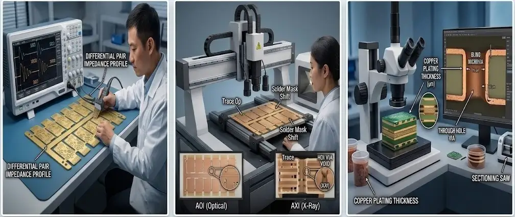
TDR Testing (Time Domain Reflectometry)
Validates precise impedance control along high-speed differential traces. We test every batch of coupons or production boards to ensure actual impedance values match design specifications within ±5% or ±10% tolerance bands. For insertion-loss-critical channels, VNA-based S-parameter verification of test coupons is available on request.
AOI (Automated Optical Inspection)
High-resolution automated inspection of every layer for trace width violations, spacing defects, shorts, opens, and solder mask issues. Catches defects invisible to the naked eye before lamination.
Automated X-Ray Inspection (AXI)
Detects inner-layer misregistration, via barrel voids, and solder joint defects in HDI blind/buried vias. Essential for verifying the structural integrity of multi-layer HDI constructions.
Microsectioning Analysis
Cross-sectional microscopic examination verifies copper plating thickness in through-holes and blind vias, dielectric thickness, and overall layer alignment — ensuring compliance with IPC-A-600 acceptance standards.
Flying Probe / Universal Electrical Test
100% continuity and isolation testing on every board. Flying probe testing is ideal for prototypes and low-volume runs; universal (fixture-based) testing provides high-throughput testing for volume production.
Solder Mask & Surface Finish Inspection
Visual and instrumental verification of solder mask coverage, ENIG/Hard Gold plating thickness (X-ray fluorescence), and gold finger bevel angle to ensure connector reliability.
Thermal Stress Testing
IPC-TM-650 thermal stress testing (solder float at 288°C) verifies the board’s resistance to thermal shock during assembly and field operation — critical for optical modules in harsh environments.
Ionic Contamination Test
Measures ionic residue on the PCB surface to ensure cleanliness meets IPC-5704 standards — preventing electrochemical migration and corrosion in high-density, high-voltage optical module applications.
Optical Module PCB Applications Across Industries
Our 6-layer optical module PCBs serve as the critical interconnect platform across a wide spectrum of optical communication and data networking applications:
Data Center Interconnects
Powering 100G/400G/800G switch-to-server connections in hyperscale data centers (AWS, Azure, Google Cloud, Meta). QSFP28/QSFP-DD transceiver modules built on our PCBs ensure reliable, low-latency data transmission across rack-to-rack and building-to-building links.
5G & Telecommunications
SFP28/SFP56 modules for 5G fronthaul (CPRI/eCPRI) and midhaul networks. Our PCBs handle the 25G/50G data rates and wide operating temperature range (−40°C to +85°C) required for outdoor base station deployments.
Long-Haul Optical Transport
CFP/CFP2/CFP4 coherent transceiver modules for DWDM long-haul and submarine cable systems. These boards support complex coherent DSP ASICs and require ultra-low-loss materials for 400G/600G/800G transmission over thousands of kilometers.
High-Performance Computing
Active Optical Cables (AOCs) and board-mounted optical engines for GPU-to-GPU and node-to-node interconnects in AI/ML clusters and supercomputers, where bandwidth density and signal integrity are paramount.
Automotive Optical Networks
Optical MOST bus and automotive Ethernet modules for in-vehicle infotainment, ADAS sensor data transmission, and autonomous driving systems. IATF 16949 certified manufacturing ensures automotive grade reliability.
Medical Imaging & Industrial
Optical imaging and industrial sensing modules — endoscopy, OCT scanners, machine vision and LiDAR — where miniaturized boards must hold tight impedance tolerances under sterilization or continuous vibration. Controlled-impedance routing and low-Dk dielectrics keep signal fidelity stable across the product service life.
Why Choose Season PCB for Your Optical Module PCB?
When it comes to high-speed optical module PCBs, manufacturing precision and engineering expertise make the difference between a reliable product and a field failure. Here’s why leading optical transceiver companies trust Season PCB:
Deep Engineering Expertise
Our engineering team has over 10 years of experience in high-speed PCB design and manufacturing. We provide free DFM (Design for Manufacturing) review on every order, identifying potential issues before production and offering optimization suggestions for impedance, stackup, and routability.
Advanced Manufacturing Equipment
State-of-the-art production lines including laser direct imaging (LDI), plasma etching, and automated plating lines ensure consistent quality from prototype to volume production. Our equipment supports the tightest tolerances in the industry.
Fast Turnaround & Flexible Volume
From 48-hour expedited prototypes to cost-efficient volume production, we scale with your needs. No minimum order quantity on prototypes. Get DFM feedback and competitive quotation within 24 hours of submitting your Gerber files.
Global Shipping & Support
We ship worldwide with DHL, FedEx, and UPS. Our customer support team is available via WhatsApp and email to answer technical questions, provide production updates, and assist with any post-delivery concerns.
Competitive Pricing
Direct factory pricing with no middleman markup. Our optimized production processes and material sourcing network deliver exceptional value — especially for mid-to-high volume production runs of optical module PCBs.
Full Documentation & Traceability
Every order includes full production documentation: stackup report, impedance test results, material certificates, COC (Certificate of Conformance), and microsection photos. Full lot traceability for quality assurance and field failure analysis.
Certifications & Compliance
Our optical module PCB production is backed by third-party certification: ISO 9001:2015 quality management, ISO 14001:2015 environmental management, and UL recognition for laminate materials (E-File E305905). IATF 16949, RoHS/REACH and GJB compliance documentation is available with your order.
Season PCB is a leading manufacturer specializing in high-speed optical interconnects. Our 6-layer optical module PCB solutions support 100G and 400G transceivers with precise impedance control, low-loss dielectric materials, and fully resin-plugged via structures.
Every panel is built under IATF 16949 and ISO 9001:2015 certified processes, with 100% electrical and AOI inspection before shipment. Fast turnaround, competitive pricing, and engineering support at every stage.
Season PCB is a specialized manufacturer of optical module PCB interconnects for next-generation data center and telecom applications, where a transceiver design leaves the least margin for error. Our process control covers fine-line imaging, multilayer lamination, and impedance verification on production coupons, so the boards you receive at 100G and 400G match the stackup you designed. Prototype samples and production volumes run through the same flow, with full DFM feedback before release.
Optical module boards that need a low-loss RF section often share the same Rogers high-frequency stackups as the radar and satellite front-ends we build them alongside.
Our designs follow IEEE 802.3 Ethernet standards and IPC manufacturing specifications. Every lot undergoes TDR impedance testing to confirm signal integrity at 100G/400G data rates. For volume production, the same stackup runs on 998PCB Group’s high-speed and high-frequency PCB lines at the group’s Shenzhen campus.
Frequently Asked Questions
Find answers to the most common questions about our 6-layer PCB for optical modules. Can’t find what you’re looking for? Contact our engineering team for personalized assistance.
Why is a 6-layer PCB preferred over a 4-layer PCB for optical modules?
A 6-layer PCB provides dedicated ground and power planes, which are essential for isolating high-speed TX/RX differential lines. This significantly reduces crosstalk, improves EMI performance, and provides cleaner power delivery (PDN) compared to a 4-layer board. The additional layers also allow for tighter impedance control and better signal integrity at data rates of 25G, 100G, and beyond. In a 4-layer board, signal and power/ground layers must share space, leading to compromised return paths and increased electromagnetic emissions — unacceptable in high-density optical transceiver applications.
What surface finish is best for the gold fingers of an optical module PCB?
Hard Gold Plating (typically 30 µ” or thicker) over Nickel is highly recommended for the edge connector (gold fingers) to ensure wear resistance over hundreds of insertion cycles. The rest of the board usually utilizes ENIG (Electroless Nickel Immersion Gold) for excellent solderability and flat surface for fine-pitch components. This dual-finish approach — ENIG for solderability + Hard Gold for connector durability — is the industry standard for optical transceiver PCBs. We also offer ENEPIG (Electroless Nickel Electroless Palladium Immersion Gold) for applications requiring wire bonding compatibility.
How do you guarantee the ±10% impedance control for high-speed differential pairs?
We use Polar Instruments (CITS800s) for pre-layout stackup simulation and run TDR (Time Domain Reflectometry) tests on every batch of coupons or boards to ensure actual impedance values match the design specifications. Our process includes: (1) Pre-production stackup simulation to verify impedance targets are achievable with the selected materials and copper weights; (2) In-process control of trace width and dielectric thickness during manufacturing; (3) Post-production TDR measurement on test coupons or actual boards. For applications requiring even tighter tolerances, we can achieve ±5% impedance control using advanced materials and precision manufacturing processes.
What materials are used for high-speed optical module PCBs?
For high-speed optical modules, we use low-loss dielectric materials including High-Tg FR4 (Tg≥170°C), Rogers RO4000 series, Panasonic Megtron 6/Megtron 7, Nelco N4000-13, and Isola. The material selection depends on the data rate requirements — for 10G applications, High-Tg FR4 is typically sufficient; for 25G modules, mid-loss materials like ITEQ or TUC are recommended; for 100G, Megtron 6 or Nelco provide the necessary low-loss performance; and for 400G+ modules, Megtron 7 or Rogers ensure minimal insertion loss at high frequencies. We also offer hybrid stackups combining different materials to optimize the cost-performance ratio.
What is the typical turnaround time for 6-layer optical module PCBs?
Standard prototype turnaround is 5–7 business days. For urgent projects, we offer expedited service with 48–72 hour turnaround (additional charges apply). Mass production typically takes 10–15 business days depending on order volume, material availability, and design complexity. DFM feedback and competitive quotations are provided within 24 hours of receiving your Gerber files and BOM.
Can you manufacture HDI 6-layer PCBs for compact optical modules?
Yes, we offer HDI (High Density Interconnect) 6-layer PCBs with blind and buried vias. Our capabilities include minimum laser-drilled microvia size of 3 mil (0.075mm) for blind vias, minimum trace width/spacing of 2/2 mil (0.050mm) with half-ounce copper, POFV (Plated Over Filled Via) technology for maximum routing density in compact SFP/QSFP form factors, and back-drilling of through-hole via stubs to protect high-speed channel bandwidth. We support 1+N+1, 2+N+2, and higher-order HDI build-ups depending on your routing density requirements.
Do you provide design support and DFM review?
Absolutely. We provide free DFM (Design for Manufacturing) review on every order. Our engineering team will check your Gerber files for manufacturability, verify stackup and impedance feasibility, identify potential issues (such as acid traps, insufficient annular rings, or impedance-critical trace geometry problems), and suggest optimizations — all before production begins. If your design needs adjustments to meet impedance targets, we’ll propose alternative stackups and material selections at no cost.
What certifications does your factory hold?
Our manufacturing facility holds the following certifications: ISO 9001:2015 (Quality Management), ISO 14001:2015 (Environmental Management), IATF 16949:2016 (Automotive Quality Management), UL recognition for laminate materials (Underwriters Laboratories — E-File E305905), and RoHS/REACH compliance. We also manufacture to IPC-6012 Class 2 as standard and can produce to IPC-6012 Class 3 for mission-critical applications upon request. GJB (Chinese military standard) production is also available for qualified defense applications.
Ready to Launch Your Next Optical Module Project?
Get expert DFM (Design for Manufacturing) feedback and a competitive quote within 24 hours.
Tel: (+86) 18681528532 (WhatsApp)
E-mail: roc@season-pcb.com