Book Appointment Now

Heavy copper PCB basics: how copper weight sets current capacity and heat spreading, what 2 to 6 oz means for etch and vias, and when the extra copper pays.
Heavy Copper PCB: Copper Weight, Current Capacity and When to Spec It
Power rails that run hot at standard copper weight, measurable voltage drop along motor drive outputs, boards that need airflow where a wider trace would have done the job — most high-current problems trace back to copper that was specified too thin. This guide explains what makes a board a heavy copper PCB, how copper weight converts into current capacity and heat spreading, which trade-offs in etch and via design come with the extra metal, and how to decide how much copper your application actually needs. Every capability number quoted here comes from our published process table — copper weights from one-third ounce up to 6 oz per layer in mass production, and up to 12 oz on sample builds after engineering review — and the selection logic below is the same one our engineering team applies when quoting power, automotive and industrial boards.
Table of Contents
- What Counts as a Heavy Copper PCB
- Copper Weight to Thickness: The Conversion Table
- How Copper Weight Sets Current Capacity
- Heavy Copper PCB Thermal and Mechanical Benefits
- Etch, Fine Lines and the Density Trade-Off
- Vias, Fills and Plugging in Heavy Copper Builds
- Heavy Copper PCB Applications and How to Choose
- What Changes on the Factory Floor
- Cost and Lead Time Expectations
- Design Checklist Before You Send Gerbers
- FAQ
- Get a Stackup Review for Your Power Board
What Counts as a Heavy Copper PCB
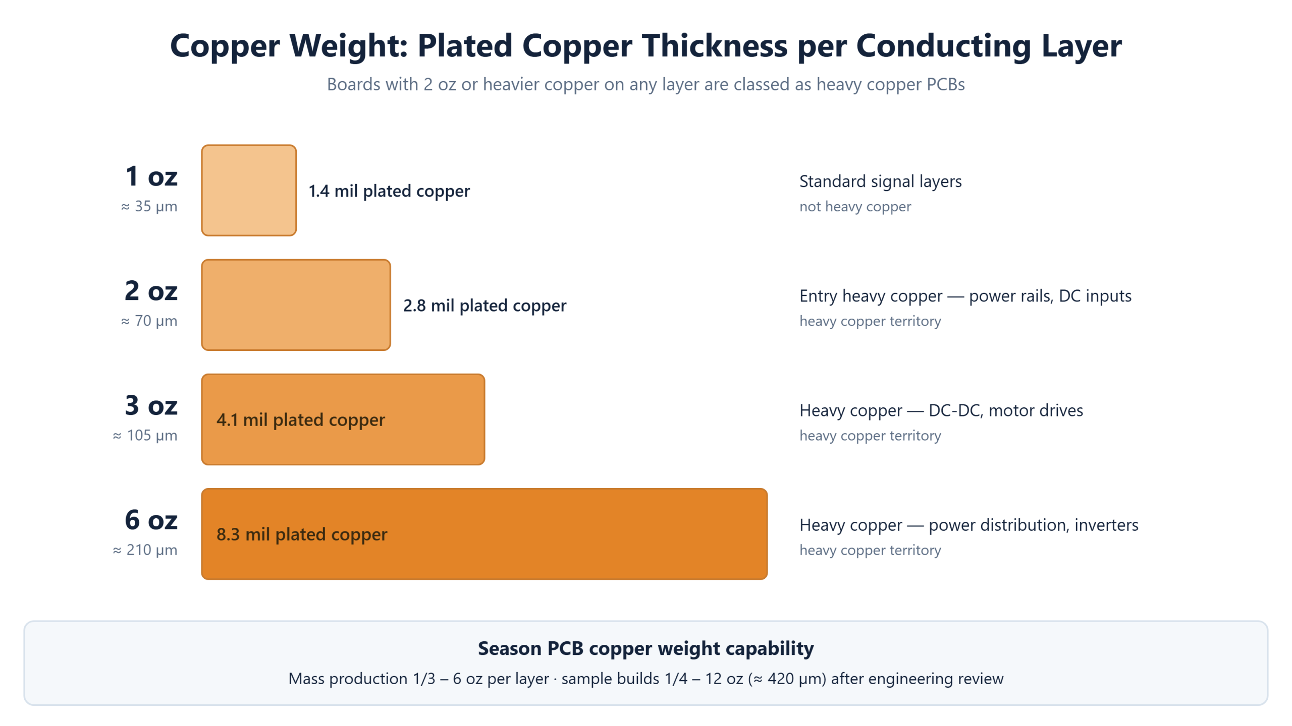
Copper weight describes how much copper sits on each conducting layer, expressed in ounces per square foot of laminate. One ounce of copper spreads into a layer roughly 35 µm (1.4 mil) thick, and that 1 oz foil is the default for signal layers on everything from consumer boards to server planes. Once any layer carries 2 oz (about 70 µm) or heavier copper, the board enters heavy copper territory; above 3 oz, fabricators usually talk about ultra-heavy copper.
The distinction matters because heavy copper changes the manufacturing conversation. Etching, plating and inspection all behave differently once the metal gets thick, and the design rules that apply to a 1 oz signal layer stop being valid. The table below summarises the practical differences before the rest of this guide works through them one by one.
| Aspect | Standard 1 oz copper | Heavy copper 2 oz and above |
|---|---|---|
| Typical role | Signal routing, light power | Power rails, current distribution, heat spreading |
| Trace cross-section at equal width | Baseline | 2× at 2 oz, 3× at 3 oz, 6× at 6 oz |
| Minimum line and spacing | Tightest values apply | Wider geometry required — confirmed per layer |
| Plating process | Single standard cycle | Extended plating-up cycles, per-cycle inspection |
| Relative board cost | Baseline | Rises step by step with copper weight |
Note that heavy copper does not have to cover the whole board. The most common builds mix weights layer by layer: 2–6 oz copper on power and ground layers, standard 1 oz on signal layers. We manufacture copper weights from 1/3 oz to 6 oz per layer in mass production, and up to 12 oz on sample builds — the range is wide enough that the real question is usually which layer gets which weight.
Copper Weight to Thickness: The Conversion Table
Because the industry quotes copper in ounces per square foot while designers think in microns or mils, the first step in any heavy copper PCB discussion is a conversion. One ounce of copper foil is approximately 35 µm thick; every additional ounce adds the same amount again. The ladder below shows the working range and where each weight typically earns its place.
| Copper weight | Plated thickness | In mil | Typical role |
|---|---|---|---|
| 1 oz | ≈ 35 µm | 1.4 mil | Standard signal layers |
| 2 oz | ≈ 70 µm | 2.8 mil | Entry heavy copper — power rails, DC inputs |
| 3 oz | ≈ 105 µm | 4.1 mil | Heavy copper — DC-DC converters, motor drives |
| 6 oz | ≈ 210 µm | 8.3 mil | Heavy copper — power distribution, inverters |
| Up to 12 oz (sample) | ≈ 420 µm | 16.5 mil | Extreme current bus structures, after engineering review |
Two footnotes keep this table honest in quotations. First, foil weight and finished plated thickness are related but not identical — plating adds copper on traces and in holes, so finished conductors measure slightly heavier than the base foil. Second, the thin end of the range matters too: foils as light as one-third ounce (≈ 12 µm) are used when fine-line signal layers need to keep impedance geometry tight. State the copper weight per layer explicitly in your fabrication notes and both sides of the conversation stay aligned.
How Copper Weight Sets Current Capacity
A trace is a resistor with a cross-section equal to its width times its copper thickness. Doubling the copper weight doubles that cross-section at the same trace width, which halves resistance and cuts I²R heating dramatically. This is the entire economic argument for a heavy copper PCB: extra metal in the stack replaces heat, voltage drop and cooling measures that would otherwise have to be designed around.
Current ratings are read from IPC-based design charts, which take trace geometry, copper thickness and the allowed temperature rise as inputs — the IPC standards family behind those charts is the shared reference across the industry. The key input is your temperature-rise budget: a trace allowed to rise 30 °C carries far less than the same trace allowed 10 °C. Decide the budget from your enclosure and airflow reality first, then read the chart.
In practice the sweet spots look like this: 2 oz comfortably handles DC inputs and power rails in the tens of amps with reasonable widths; 3–4 oz is the default for motor drives and DC-DC stages; 6 oz and beyond serve distribution layers where many high-current branches share one plane. Whatever the target, our engineering team verifies the trace-and-via arithmetic against the chosen temperature rise before quotation — the review is where optimistic assumptions usually get corrected.
Heavy Copper PCB Thermal and Mechanical Benefits
Thick copper does two jobs beyond carrying current. As a thermal path, heavy planes act as in-plane heat spreaders: they pull heat away from power devices and distribute it toward mounting holes, thermal vias and the board edge, flattening the hotspots that thin-copper layouts develop around regulators and switches. For power boards that cannot justify exotic substrates, moving from 1 oz to 3 oz planes is often the single most effective thermal change available.
Mechanically, the extra metal shows up where boards take abuse. Heavier copper gives plated holes and component pads more cross-section, which tolerates vibration and repeated temperature cycling better — one reason automotive power and body-electronics boards routinely specify 2 oz or more. Our 4-layer automotive PCB platform is a typical example of the weight class that keeps connectors and high-power components anchored over the life of a vehicle.
Both benefits scale with placement, not just thickness. A 3 oz plane only helps if it actually connects the heat source to something that can move heat onward — mounting hardware, thermal vias, or a metal enclosure interface. When we review a heavy copper PCB stackup, the thermal questions are about continuity of the path, and the mechanical ones are about where the board flexes. Copper weight is the enabler; geometry decides how much of the benefit you collect.
Etch, Fine Lines and the Density Trade-Off
Etching removes copper downward and sideways at the same time. With 1 oz foil the sideways attack is small; with 6 oz it is deep enough to shape the trace walls noticeably and to require much wider minimum lines and spaces. The practical rule: as copper weight rises, achievable feature density falls. A layer that routes 4/4 mil geometry at 1 oz may need several times that spacing at 4 oz, so heavy copper layers should be planned as coarse, high-current structure rather than fine routing.
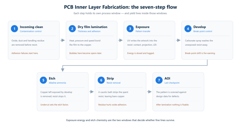
This is why mixed-weight stackups are the standard answer. Power layers carry the heavy copper with generous geometry; signal layers keep 1 oz (or lighter) and their tight minimums — our production minimum line and spacing is 2/2 mil on inner layers — untouched. Laser direct imaging keeps the etch masks accurate across the weight range, and the inner-layer imaging, etch and AOI flow described in our inner layer fabrication guide runs the same way for both.
When you plan a mixed build, put the heavy layers where they have room: power distribution and ground planes rarely need fine features anyway. The layouts that struggle are the ones asking a 4 oz layer to also break out fine-pitch BGA fanouts — that job belongs on a standard-weight layer with vias carrying the current down to the power structure.
Vias, Fills and Plugging in Heavy Copper Builds
Current that flows on heavy layers still has to change layers, and the via becomes the bottleneck. A via barrel is a thin copper tube compared with the planes it joins, so power paths through vias need either many parallel holes or deliberately filled and capped structures. We offer via-in-pad with conductive via fill as a standard special process, and the plating and filling mechanics are covered in detail in our copper-filled vias guide.
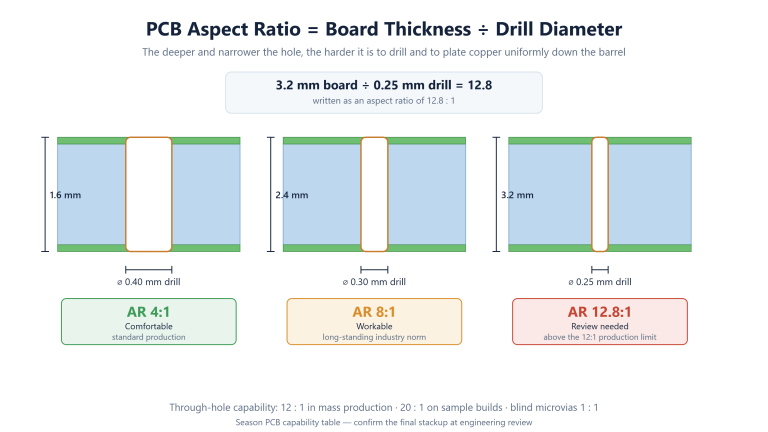
Heavy copper boards tend to be thick boards, and thickness pulls the hole geometry into the ratio discussion: a 3.2 mm stack with 0.3 mm drills sits at 10.7:1, close enough to the production limit that it deserves an explicit check. Our PCB aspect ratio guide walks through that calculation and the plating limits behind it, which matter even more when the same panel carries heavy plating cycles.
Solder mask and surface finish also behave differently over thick conductors. The steeper trace walls of heavy copper need slightly generous mask openings, and pad-heavy power layouts give surface finishes more metal to cover. None of this is exotic — ENIG, OSP, HASL and immersion finishes all run on heavy copper panels daily — but it is one more reason the stackup should be reviewed as a whole rather than layer by layer.
Heavy Copper PCB Applications and How to Choose
Applications choose their copper weight from three inputs: steady-state current, allowed temperature rise, and the mechanical environment. The matrix below collects the weight classes we see most often in production, and the reasoning behind each — use it as a starting point, then let the current charts and an engineering review settle the exact number.
| Application | Typical copper weight | Why this class |
|---|---|---|
| DC-DC converters and power modules | 2–3 oz | Resistive loss and voltage drop at sustained current |
| Motor drives and industrial controls | 3–6 oz | High current plus vibration and thermal cycling |
| Solar and wind inverters | 3–6 oz | Surge currents and heat spreading outdoors |
| Automotive power distribution and lighting | 2–4 oz | Reliability under vibration and wide temperature swings |
| Server and telecom power backplanes | 2–3 oz | Distributed power across many slots with modest per-trace width |
Industrial boards illustrate the logic end to end: our 10-layer HDI industrial control PCB class of products combines standard-weight HDI signal structure with the heavier power layers the application demands, in one laminated stack. The pattern generalises — heavy copper is rarely a whole-board decision, it is a per-layer decision that the rest of the stack supports.
One selection habit prevents most regrets: specify from the temperature-rise budget backward, not from the copper weight forward. Boards specified as “6 oz everywhere” often carry cost that no current path uses, while boards specified at 2 oz with a 40 °C rise assumption run hotter than the enclosure can tolerate. The budget-first approach lands on the right weight and documents why.
What Changes on the Factory Floor
A heavy copper PCB runs the same backbone process as any multilayer board — imaging, etch, lamination, drilling, plating, mask, finish, test — but several steps stretch. Plating-up to 3 oz and beyond happens in controlled cycles, with copper thickness and uniformity inspected after each one. Etch and outer-layer AOI get stricter because a defect in thick copper costs more to rework. And lamination carries more copper mass per panel, which our lamination process guide shows is already the most parameter-sensitive step in multilayer manufacturing.
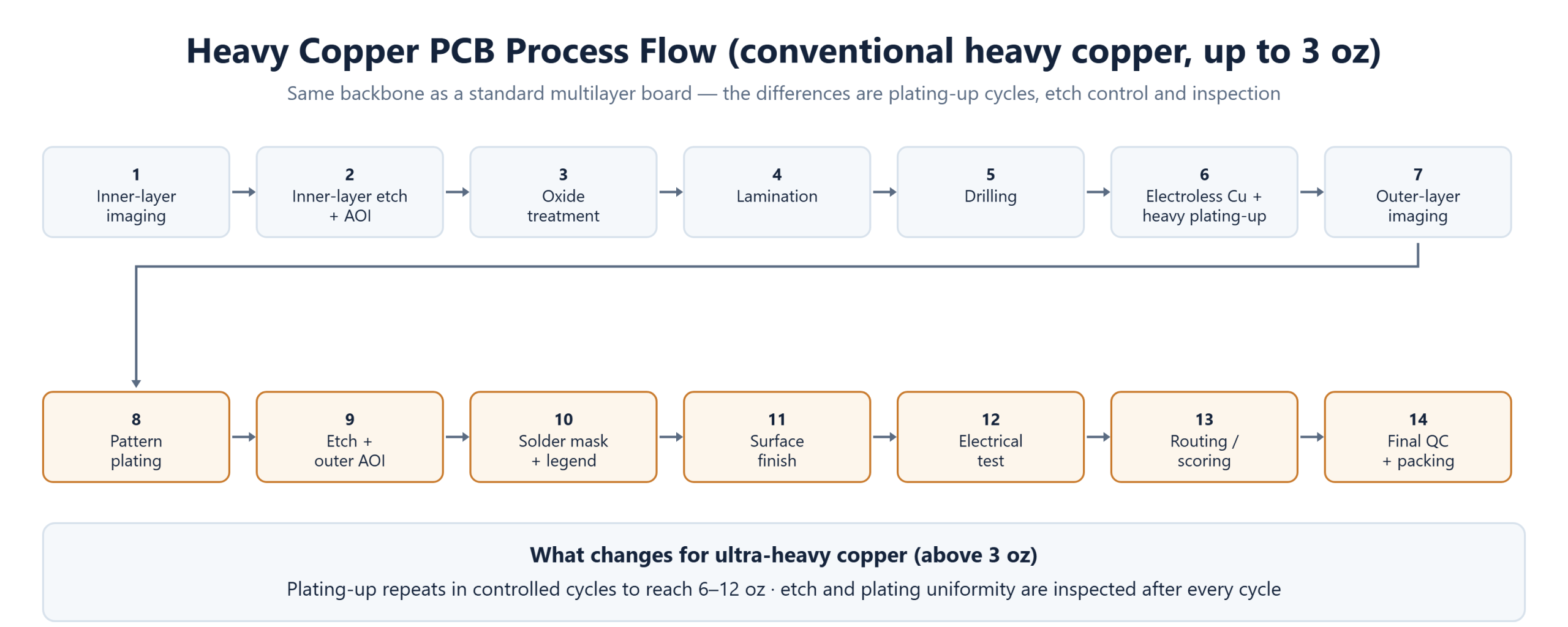
For ultra-heavy copper above 3 oz, the plating-up repeats continue until the target weight is reached, which is why those builds sit in our sample capability and are quoted after engineering review. The flow diagram above shows the full sequence for conventional heavy copper — fourteen steps, with the differences from a standard build concentrated in plating, etch control and inspection rather than in any new machinery.
Cost and Lead Time Expectations
Copper weight drives cost through material, process time and yield, in that order. Heavier foil costs more, plating-up cycles consume bath time and inspection, etch runs slower, and thick-copper panels leave less room for rework. Each step up the ladder — 1 oz to 2 oz to 3 oz — typically adds a meaningful percentage to the board price rather than a flat surcharge, and the exact figure depends on how much of the board carries the heavy layers.
Lead time follows the same logic: a heavy copper prototype usually takes a few working days longer than the same layer count at standard weights, with builds above 3 oz quoted individually after engineering review. The habit that keeps quotations comparable is simple — ask every supplier to state the copper weight per layer on the quote, the same way thickness and finish are stated. A heavy copper PCB quoted without that line is a quotation you cannot compare.
Finally, remember that copper weight is one of the few specifications where over-specification is visible and correctable. If a quotation comes back high, the first question worth asking is whether every heavy layer actually carries current that needs it — consolidating power onto fewer, well-planned heavy layers frequently trims cost without touching electrical performance.
Design Checklist Before You Send Gerbers
Heavy copper rewards a little preparation at design time with a much smoother quotation and build. Before releasing Gerber data on a power board, run through this list — each line maps to a question our CAM engineers would otherwise ask anyway.
- State the copper weight per layer in the fabrication notes, not just in the stackup table
- Check minimum line and spacing per layer against its copper weight — heavy layers need wider geometry
- Verify that via current share matches the trace ratings, and call out fills or plugging where vias sit in power paths
- Keep stackup symmetry and copper balance so lamination stays flat
- Fix the temperature-rise budget before reading current charts, and record it
- Send the stackup for engineering review early enough that weight changes are still cheap
Pair the checklist with the material side of the decision — foil weight interacts with laminate choice, glass styles and resin content, all covered in our laminate selection guide and on the PCB materials and laminates hub. Copper weight and laminate are chosen together, and the review that confirms one should confirm the other.
Frequently Asked Questions
What copper weight counts as a heavy copper PCB?
Any board with 2 oz or heavier copper on at least one layer. Standard production boards use 1 oz (about 35 µm) on signal layers; heavy copper starts at 2 oz (about 70 µm) and fabricators usually call 3 oz and above ultra-heavy. Our production range runs from one-third ounce up to 6 oz per layer, with 12 oz available on sample builds.
How much current can a heavy copper PCB carry?
It depends on trace width, copper weight and the allowed temperature rise. Readings come from IPC-based charts: doubling copper weight doubles the cross-section at the same width and roughly halves the resistive heating. Decide the temperature-rise budget first — a 10 °C allowance carries far less than 30 °C — then read the chart for your geometry.
What is the practical difference between 2 oz and 3 oz copper?
Cross-section and cost. At the same trace width, 3 oz carries about 50% more current than 2 oz and dissipates less heat along the same path, while adding plating time and etch constraints. Boards that sit at 2 oz with a comfortable temperature margin gain little from 3 oz; boards already running warm near their limits usually do.
Can heavy copper and fine-line routing coexist on one board?
Yes, and it is the standard approach. Power and ground layers carry 2–6 oz copper with generous geometry, while signal layers keep 1 oz or lighter and their tight minimum line and spacing. What does not work well is asking a single heavy layer to also route fine-pitch features — etch geometry will not allow it.
Does a heavy copper PCB cost significantly more?
Cost rises step by step with copper weight through foil, plating and etch time, and heavy layers reduce rework room, which affects yield. The increase is meaningful but gradual — usually a percentage step per weight class rather than a doubling. Stating copper weight per layer on the quotation is the only way to compare prices accurately.
Which surface finish should I choose for heavy copper boards?
All the common finishes run on heavy copper: ENIG, OSP, HASL, immersion silver and immersion tin, plus hard gold for connector edges. The choice follows the same logic as any board — solderability, shelf life and contact requirements. Heavy copper mainly affects pad geometry and mask openings, not the finish chemistry itself.
How thick can heavy copper plating go?
Our mass production range reaches 6 oz (about 210 µm) per layer; sample builds can extend to 12 oz (about 420 µm) after engineering review. Above 3 oz the plating-up runs in controlled cycles with thickness verified after each pass, which is why those builds are quoted individually rather than from a standard price table.
Get a Stackup Review for Your Power Board
Send us your Gerber data and target currents, and our engineering team will map the copper weight per layer, verify the trace and via arithmetic against your temperature-rise budget, and flag the layers where heavy copper earns its cost. The review happens before quotation, so the price you receive already reflects the copper your board actually needs.