Book Appointment Now

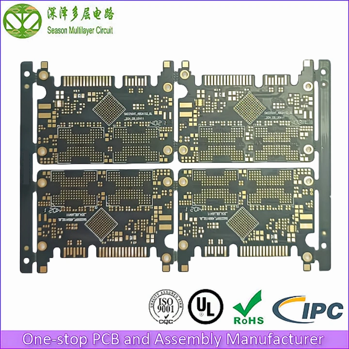
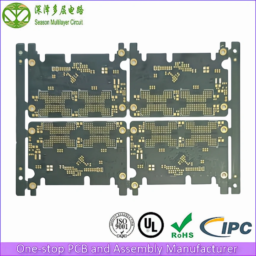
Custom 4-Layer SATA SSD PCB Manufacturing
This 4-layer SATA SSD PCB is engineered for SATA III 6 Gbps solid-state drives — optimizing signal integrity, thermal dissipation, and long-term durability for consumer and industrial storage, with strict 50Ω/85Ω/100Ω impedance control and 3/3mil fine-pitch routing.
Built on FR-4 Tg 180 with ENIG surface finish, every SATA SSD PCB undergoes 100% electrical testing and impedance verification before shipment. For urgent builds, our fast PCB manufacturing services offer expedited turnaround.
4
Layer Count
4/4 mil
Min. Trace / Space
0.20 mm
Min. Via Diameter
Tg 180
Glass Transition Temp
1 µ”
ENIG Gold Thickness
ISO 9001:2015
ISO 14001
UL (E305905)
IPC Class 2 / Class 3
IATF 16949
RoHS
4-Layer SATA SSD PCB Stackup Diagram
Proper layer ordering is critical to prevent impedance mismatching. Our standard 1.0mm thickness stackup includes dedicated signal, ground, and power layers optimized for SATA III 6Gbps performance.
- Top Layer (Signal): Component placement, high-speed SATA differential pairs, and local power routing.
- Layer 2 (Ground Plane): Solid reference ground to minimize EMI and provide a return path for high-speed signals.
- Layer 3 (Power Plane): Dedicated power distribution for VCC, VCCQ, and core voltages.
- Bottom Layer (Signal): NAND Flash routing and secondary components.
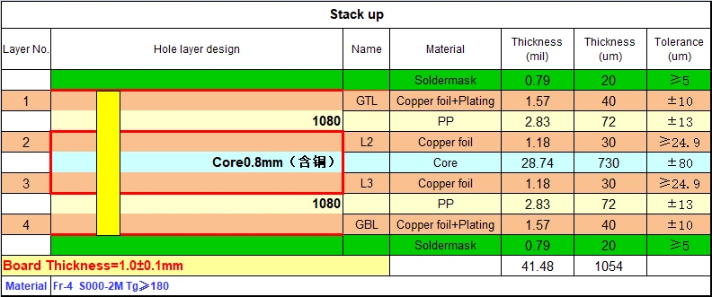
If your design’s trace width and spacing fall short of strict impedance tolerances, don’t worry. We proactively optimize your original Gerber files to ensure your boards perform exactly as intended — adjusting trace geometry, dielectric thickness, and copper weight for optimal manufacturing stability.

Technical Capability & Specifications
| Parameter | Specification | Advanced Capabilities |
|---|---|---|
| Layer Count | 4 layers | 2–32L (mass); 2–64L (sample) |
| Base Material | FR-4 S1000-2M Tg 180 | SY, NY, TUC, ZY, EMC, KB, ITEQ, Rogers, Megtron, Nelco, Isola |
| Board Thickness | 1.0mm | 0.2–6.4mm (mass); 0.15–20mm (sample) |
| Panel Size | 122.75 × 82mm / 4-up | 800 × 600mm (mass); 1050 × 610mm (sample) |
| Copper Thickness | Outer: 1 oz Inner: 1 oz | Outer: 1/3–12 oz Inner: 1/4–12 oz |
| Min Drill Size | 0.2mm | 0.15mm (mass); 0.127mm (sample) |
| Min Trace Width/Spacing | 3/3 mil | 2.5/2.5 mil (1 oz) 2/2 mil (0.5 oz) |
| Min BGA Pad | 0.3mm | 0.15mm |
| Surface Finish | ENIG 1–2 µ” | OSP, ENIG, HASL, Electric Hard Gold, ENIG+OSP, ENEPIG, Immersion Silver & Tin |
| Solder Mask Color | Matte Black | Green, Blue, Black, White, Yellow, Red, Purple, Matte Green, Matte Blue, Matte Black |
| Impedance Control | ±10% (50/85/100Ω) | ±5% (Strict Tolerance) |
| Min Routing Tolerance | ±0.15mm | ±0.075mm |
| Quality Standard | IPC Class 2, RoHS | IPC Class 3, UL, RoHS, IATF 16949, GJB |
| PCB Type | Multilayer | HDI, Multilayer, Rigid-Flex, High Frequency, High Speed, Hybrids & Mixed Dielectrics |
Engineered for High-Speed Storage Performance
A 4-layer PCB stackup is the industry-standard sweet spot for SATA III (6Gbps) SSDs, offering an ideal balance between manufacturing cost-efficiency and robust electromagnetic interference (EMI) shielding. Our premium 4-layer SATA SSD PCBs are fully optimized for leading controller architectures—including SMI, Phison, and Marvell—ensuring seamless compatibility and high-speed data transmission with 3D TLC/QLC NAND Flash memory.
Optimized Signal Integrity
Our standard Signal-Ground-Power-Signal layout provides a solid reference ground plane. This design minimizes cross-talk, controls impedance mismatch, and ensures an ultra-low noise floor for high-frequency data tracks at 6Gbps.
Advanced Thermal Management
To prevent thermal throttling during continuous heavy read/write workloads, we implement dense arrays of thermal vias directly beneath the SSD controller and Power Management IC (PMIC). Vias are plated and, where the stack-up allows, filled and capped so the pad stays flat for BGA soldering. Combined with 1 oz outer copper and a solid ground plane, heat spreads across the board instead of concentrating under one package, keeping the controller inside its operating window during sustained transfers.
Precision Impedance Control
Strict 50Ω (single-ended), 85Ω (differential), and 100Ω (differential) impedance control with ±5% strict tolerance available. Every batch ships with a dedicated Polar Instruments impedance testing report.
Premium Material Selection
Standard FR-4 S1000-2M with Tg 180 for excellent thermal stability, supplied as UL 94 V-0 rated laminate with matching prepreg so that core and bond-ply come from the same material family and the cured stack-up behaves predictably. Also available in Rogers, Megtron, Nelco, and Isola for high-frequency and mixed-dielectric applications.
ENIG Surface Finish
Electroless Nickel Immersion Gold provides a perfectly flat surface for fine-pitch BGA components, which is critical for SSD controllers and NAND Flash packages. A typical 3–6 micron nickel layer with 0.05–0.1 micron gold keeps every pad coplanar, so paste release and joint formation stay consistent across hundreds of balls. The gold layer also resists oxidation, which matters for storage modules that may sit in inventory for months before assembly.
Data Integrity at 6 Gbps
At 6 Gbps a single impedance discontinuity is enough to corrupt a data burst, so signal integrity is treated as a build parameter rather than an inspection item. Differential pairs are routed with matched lengths, reference planes stay continuous under the controller and connector footprints, and impedance coupons are placed on every production panel so the stack-up can be verified on the boards that actually ship.
Applications of 4-Layer SATA SSD PCBs
Our high-reliability storage PCBs are widely deployed across various storage form factors and market segments worldwide.
2.5-Inch Consumer SSDs
Cost-effective designs optimized for standard laptop and desktop upgrades, with high-volume production and consistent quality for retail and OEM channels. The 2.5-inch SATA drive remains the default upgrade path for legacy notebooks and desktop refreshes, where a 4-layer stack-up keeps unit cost competitive while still meeting the SATA III signal requirements.
Where the design moves on to a USB 3.2 or USB4 portable enclosure, the same SSD routing discipline scales onto a 10-layer portable SSD PCB with a 1.0 mm FR4 Tg 170 stack.
Industrial Storage Modules
Enhanced thermal resistance for rugged computing, automotive data logging, and industrial storage. Wide-temperature SSD modules have to stay stable across the full operating range, so we specify Tg 180 FR-4 or higher-grade laminates and balance copper distribution to limit warpage and keep the assembly reliable under vibration.
Embedded Systems
mSATA, M.2 SATA (B and M key) and other small-form-factor storage for IoT gateways, POS terminals, and embedded computing platforms where space and reliability are critical. These modules usually carry the controller and NAND on a compact outline, so fine-pitch routing, controlled impedance and via-in-pad capability matter more than raw layer count.

Our Quality Guarantee for Storage PCBs
SATA III operates at 6Gbps — even minor manufacturing defects can cause data corruption. We implement rigorous testing protocols to ensure every board meets the highest standards.
100% AOI & E-Test
Automated Optical Inspection and Flying Probe / Fixture Testing for all layers. No board ships without passing full electrical testing.
Controlled Impedance Test
A dedicated Polar Instruments impedance testing report is provided with every batch, guaranteeing signal integrity compliance.
International Certifications
Fully certified to ISO 9001:2015, ISO 14001, UL (E305905), and RoHS standards. IPC Class 3 is available on request for mission-critical applications, with acceptance criteria per IPC-A-600. For background on what the UL marking covers, see our guide to UL certified PCB standards.
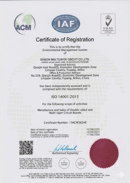
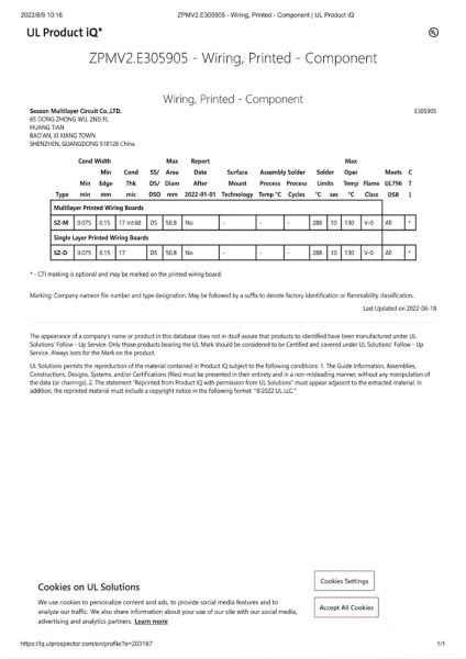
Our SATA SSD PCB designs comply with SATA-IO specifications and IPC manufacturing standards. These SATA SSD PCB boards undergo full electrical testing to ensure signal integrity and storage reliability. The same build scales to high volumes on 998PCB Group’s 2–30 layer PCB lines at the group’s Shenzhen campus.
Frequently Asked Questions
Why use a 4-layer PCB instead of a 2-layer PCB for a SATA SSD?
SATA III operates at a high frequency of 6 Gbps. A 2-layer board cannot provide the required solid reference ground plane, leading to massive EMI, signal degradation, and data loss. A 4-layer PCB provides dedicated ground and power layers to ensure stable signal integrity.
What surface finish is best for a 4-Layer SATA SSD PCB?
ENIG (Electroless Nickel Immersion Gold) is highly recommended. It provides a perfectly flat surface for fine-pitch BGA components (like Flash and controllers) and offers excellent oxidation resistance for storage devices.
Do you support reverse engineering or custom PCB layout from a schematic?
Yes, we provide full ODM and OEM services. If you have the SSD controller schematic or an existing sample, our engineering team can design the 4-layer PCB layout for you.
What is the lead time for a 4-layer SATA SSD PCB order?
Lead time depends on layer count, surface finish, impedance class and the capacity available at the time of order. Prototype and volume builds follow different bands. Our PCB lead time page lists the standard schedule, and if you are working to a fixed date we will confirm feasibility when we quote.
What determines the price of a 4-layer SATA SSD PCB?
The main drivers are board size and panel utilisation, laminate grade, copper thickness, surface finish, impedance tolerance class, quantity and schedule. A standard Tg 180 FR-4 build with ±10% impedance control sits at the entry point, while low-loss laminates, ±5% tolerance or an expedited schedule cost more. Our guide to the components of PCB prices breaks each factor down.
Should I choose ±10% or ±5% impedance tolerance?
±10% covers the majority of SATA III designs at lower cost. Choose ±5% when the controller vendor specifies a tighter window, when trace geometry is unusually narrow, or when the design sits at the edge of the stack-up capability. We confirm which class your design needs during the DFM review and quote the matching tolerance.
Ready to start your 4-Layer SATA SSD PCB project?
Upload your Gerber files for an instant PCB quote and get an engineered review within 24 hours.
Tel: (+86) 18681528532 (WhatsApp)
E-mail: roc@season-pcb.com