Book Appointment Now

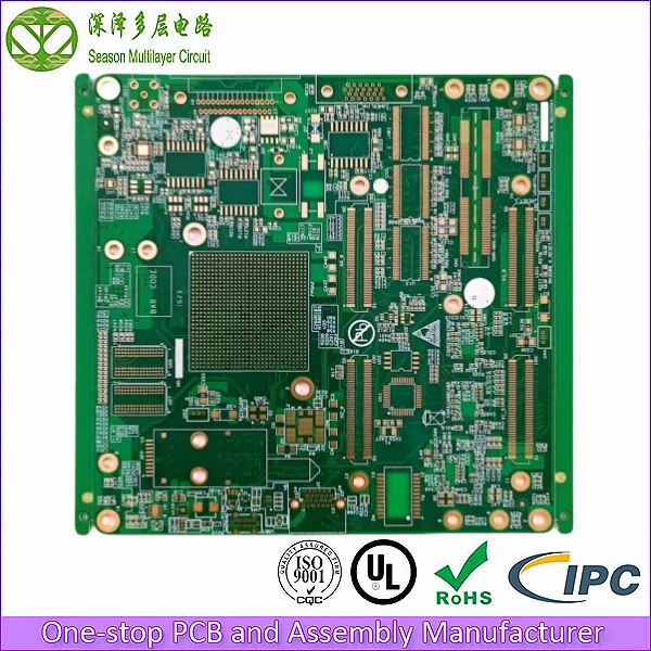
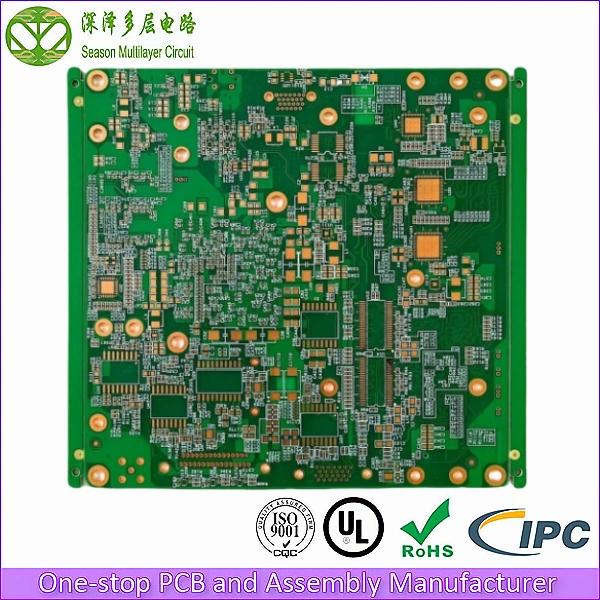
14-Layer Computing PCB
Ultra-high-density 14-layer computing PCBs for high-performance computing platforms, AI accelerators, and edge computing systems with multi-gigabit memory interfaces, dense BGA routing, and advanced thermal management for sustained compute workloads.
High-performance computing systems demand PCBs that can route multi-gigabit memory interfaces (DDR5, HBM), PCIe Gen5 links, and dense BGA fanouts — all while managing extreme thermal loads from power-hungry processors. At Season Multilayer Circuit, we manufacture 14-layer computing PCBs with HDI technology, back-drilling,, back-drilling, and heavy copper thermal management for AI, data center, and edge computing applications.
14
Layer Count
3/3 mil
Min. Trace/Space
0.10 mm
Min. Via Diameter
Tg 180
Glass Transition Temp
1–2 µ”
ENIG Gold Thickness
ISO 9001:2015
ISO 14001
UL (E305905)
IPC Class 2 / Class 3
RoHS
14-Layer Computing PCB Stackup Diagram
Our 14-layer stackup for high-performance computing applications provides comprehensive signal integrity, multi-domain power distribution, and thermal management for AI accelerators, server motherboards, and edge computing platforms.
- Top Layer (Copper/Plated): CPU/GPU BGA, memory modules, high-speed I/O
- Inner Layer 2 (Ground Plane): Reference for L1 high-speed memory signals
- Inner Layer 3 (Signal Layer): DDR5/DDR4 memory interface routing
- Inner Layer 4 (Ground Plane): Signal reference and EMI shielding
- Inner Layer 5 (Signal Layer): PCIe Gen4/Gen5 differential pair routing
- Inner Layer 6 (Power Plane): Core voltage distribution (VCORE)
- Inner Layer 7 (Ground Plane): Power reference and thermal spreader
- Inner Layer 8 (Power Plane): Memory voltage (VDDQ) and I/O power
- Inner Layer 9 (Ground Plane): Signal reference for L10
- Inner Layer 10 (Signal Layer): High-speed SerDes and networking interfaces
- Inner Layer 11 (Signal Layer): Low-speed control and management signals
- Inner Layer 12 (Ground Plane): Bottom signal reference
- Inner Layer 13 (Power Plane): Auxiliary power distribution
- Bot Layer (Copper/Plated): Bottom BGA routing and thermal pad
The 14-layer architecture provides five ground planes and three power planes, creating a low-impedance power delivery network (PDN) essential for high-performance processors. Back-drilling on signal vias enables multi-gigabit memory and PCIe signal integrity. The FR-4 S1000-2M substrate provides good thermal stability and electrical properties, while the ENIG surface finish ensures reliable soldering of fine-pitch BGA packages.
Technical Capability & Specifications
| Parameter | Specification | Advanced Capabilities |
|---|---|---|
| Layer Count | 14 Layer | 2-32L (Mass); 2-64L (Sample) |
| Base Material | FR-4 S1000-2M Tg 180 | SY, NY, TUC, ZY, EMC, KB, ITEQ, Rogers, Megtron, Nelco, Isola |
| Board Thickness | 2.4mm | 0.2-6.4mm (Mass); 0.15-20mm (Sample) |
| Panel Size | 200x180mm/1 | 800x600mm (Mass); 1050×610 (Sample) |
| Copper Thickness | Outer: 1 oz Inner: 1 oz | Outer: 1/3–12 oz Inner: 1/4–12 oz |
| Min Drill Size | 0.10mm (Laser) | 0.075mm (Laser Sample) |
| Min Trace Width/Spacing | 3/3 mil | 2.5/2.5 mil (Sample) |
| Back-Drill | Available (+/-0.05mm) | Min stub: 0.10mm |
| Surface Finish | ENIG | ENIG, ENEPIG, OSP, Immersion Silver |
| Solder Mask | Green | Green, Black, Blue, Red, Yellow, White, Purple |
| Impedance Control | 40/50/85/100 Ohm +/-8% | +/-5% available for memory interfaces |
| BGA Pitch Support | 0.4mm | 0.3mm (Sample) |
Key Advantages of Our 14-Layer Computing PCB
- 5-Ground-Plane PDN Architecture: Five dedicated ground planes create a low-impedance power delivery network, reducing power supply noise by 20dB+ for stable high-performance processor operation at sustained loads.
- HDI BGA Fanout Capability: 0.10mm laser-drilled blind vias with 3/3 mil trace/space enable dense fanout routing for 0.4mm pitch BGAs used in modern CPUs, GPUs, and AI accelerators.
- Back-Drilled Multi-Gigabit Channels: Back-drilling on signal vias eliminates stub reflections, enabling clean DDR5 and PCIe Gen4/Gen5 signal transmission at 16+ Gbps data rates.
- Multi-Domain Power Isolation: Separate power planes for core voltage (L6), memory voltage (L8), and auxiliary power (L13) prevent cross-domain noise coupling in mixed-voltage computing systems.
- Heavy Copper Thermal Option: Available 2-12 oz inner copper for thermal spreading under high-TDP processors, reducing junction temperatures by 15-20C compared to standard copper weights.
Overcoming Critical Challenges in High-Performance Computing Design
When sourcing PCBs for high-performance computing applications, engineers encounter three critical challenges. Here is how our engineering team eliminates them:
1. DDR5 Memory Signal Integrity at 6400+ MT/s
The Problem: DDR5 memory interfaces operate at 6400 MT/s and beyond, requiring precise impedance control, minimal crosstalk, and clean signal paths. Poor PCB design causes setup/hold violations, bit errors, and memory training failures that prevent system boot.
Our Solution: Our 14-layer stackup places DDR5 signal layers (L3) between dedicated ground planes (L2, L4) for optimal signal reference. Tight impedance control (40 ohm single-ended, 85 ohm differential at +/-8%) and length matching (within +/-5mil) ensure clean memory signals. Back-drilled vias eliminate stub reflections at connector transitions.
2. Thermal Management for High-TDP Processors
The Problem: Modern AI accelerators and server CPUs dissipate 300-500W, creating extreme thermal density. Standard PCB copper weights cannot spread this heat effectively, causing local hotspots that degrade performance and trigger thermal throttling.
Our Solution: We offer heavy inner copper (up to 12 oz) on dedicated thermal layers connected to the processor via thermal via arrays. The multiple ground planes act as thermal spreaders, distributing heat across the board. For extreme thermal loads, we offer copper coin inlays and metal-core substrate options.
3. Dense BGA Fanout for 0.4mm Pitch Processors
The Problem: Modern CPUs and AI accelerators use 0.4mm pitch BGA packages with thousands of pins. Routing escape patterns from these dense arrays requires HDI technology that conventional PCBs cannot provide.
Our Solution: Our HDI process with 0.10mm laser-drilled blind vias and 3/3 mil trace/space enables full fanout of 0.4mm pitch BGAs. Via-in-pad technology (with resin fill and copper planarization) places interconnects directly under BGA pads, maximizing routing channels. For 0.3mm pitch, we offer 0.075mm laser microvias.
Where Our Computing PCBs Are Used
Our 14-layer computing PCBs power a wide range of high-performance computing applications:
- AI Accelerator Cards: GPU/TPU accelerator boards with PCIe Gen5 interfaces for machine learning training and inference in data centers.
- Edge Computing Platforms: Compact edge servers with AI inference capability for industrial IoT, smart cities, and autonomous systems.
- Server Motherboards: High-density server motherboards with multi-socket CPU configurations, DDR5 memory, and PCIe expansion.
- Network Processing Units: High-throughput network processing boards with 100/400G Ethernet and hardware-accelerated packet processing.
- High-Performance Storage Controllers: NVMe SSD controller boards with PCIe Gen4/Gen5 interfaces for enterprise storage systems.
Our Quality Guarantee for Computing PCBs
High-performance computing electronics demand exceptional signal integrity and thermal reliability. We implement rigorous testing protocols on every board:
- 100% AOI Inspection: Automated Optical Inspection scans every layer for trace breaks, shorts, and alignment errors.
- 100% Electrical Testing (E-Test): Fixture-based testing with high-density probe arrays for BGA pin verification.
- Controlled Impedance Testing: Polar Instruments test report documenting 40/50/85/100 ohm compliance.
- Back-Drill Verification: Cross-section inspection of back-drilled via stub length on sample boards.
- Certifications: ISO 9001:2015, ISO 14001, UL (E305905), RoHS compliant. IPC Class 3 available for enterprise computing.
Why Choose Season PCB for Your Computing PCB?
With nearly 20 years of experience in PCB manufacturing, Season Multilayer Circuit has served over 8,000 global clients in high-performance computing, data centers, and telecommunications. Our three manufacturing facilities provide capacity for both rapid prototyping and high-volume production.
We understand that high-performance computing electronics demand exceptional signal integrity and thermal management. That is why every 14-layer computing PCB we ship is backed by:
- Free DFM file checking before production — including signal integrity review
- 24/7 dedicated engineering support
- Guaranteed on-time delivery
- No minimum order quantity — from 1 prototype to 50,000+ units
- Engineering fee waivers on bulk production orders
Season PCB specializes in 14-layer computing PCB manufacturing for AI accelerators and high-performance computing platforms and edge computing platforms. Our computing PCB products feature 5-ground-plane PDN architecture, HDI BGA fanout, and back-drilled multi-gigabit channels. We also manufacture high-speed backplane PCBs and 10-layer M.2 SSD PCBs for computing applications. Each computing PCB meets IPC standards.
For your 14-layer computing PCB needs, Season PCB provides fast turnaround, competitive pricing, and ISO-certified quality. Explore our PCB manufacturing capabilities or contact us for computing PCB manufacturing today.
Our computing PCB boards comply with UL safety certifications, IPC manufacturing standards, and JEDEC memory specifications for DDR5 and HBM. Each computing PCB undergoes signal integrity testing per IEEE standards and thermal verification. Volume programmes of this build run on 998PCB Group’s 2–30 layer PCB lines under the same quality system.
Frequently Asked Questions
What BGA pitch sizes can your 14-layer PCBs support?
Our standard HDI process supports 0.4mm pitch BGAs using 0.10mm laser-drilled blind vias with 3/3 mil trace/space. For sample production, we can support 0.3mm pitch using 0.075mm laser microvias and 2.5/2.5 mil trace/space. Via-in-pad technology is available for maximum routing density.
Can you provide back-drilling on 14-layer boards?
Yes, we provide controlled-depth back-drilling with +/-0.05mm depth accuracy. Minimum achievable stub length is 0.10mm. Back-drilling is recommended for all multi-gigabit signal vias (DDR5, PCIe Gen4/Gen5, SerDes) to eliminate stub-induced signal reflections.
What is the lead time for 14-layer HDI computing PCB prototypes?
Standard 14-layer HDI prototype lead time is 10-14 working days due to the complex sequential lamination and back-drilling processes. Expedited 7-day service is available. Mass production typically takes 18-25 working days.
What materials and processes are available for 14-layer computing PCBs?
The standard build is FR-4 S1000-2M (Tg 180) at 2.4mm board thickness, with SY, NY, TUC, ZY, EMC, KB, ITEQ, Rogers, Megtron, Nelco, and Isola laminates available. Copper is 1 oz outer and 1 oz inner, expandable to 12 oz. Minimum laser drill is 0.10mm with 3/3 mil trace width and spacing, and back-drilling is held to +/-0.05mm with a minimum stub of 0.10mm. ENIG is the standard surface finish, with ENEPIG, OSP, and immersion silver optional. Solder mask is green as standard, with black, blue, red, yellow, white, and purple available. Controlled impedance covers 40/50/85/100 ohm at +/-8%, with +/-5% available for memory interfaces, and BGA pitch support starts at 0.4mm.
How do you verify quality on 14-layer computing PCBs?
Every board passes 100% AOI, which scans each layer for trace breaks, shorts, and alignment errors, plus 100% electrical testing on fixture-based systems with high-density probe arrays for BGA pin verification. A Polar Instruments impedance test report documenting 40/50/85/100 ohm compliance accompanies every batch, and cross-section inspection verifies back-drilled via stub length on sample boards. We are certified to ISO 9001:2015, ISO 14001, UL (E305905), and RoHS, with IPC Class 3 available for enterprise computing.
Ready to start your Computing PCB project?
Whether you need 5 pieces for prototyping or 50,000 for mass production, our engineering team is ready to support your computing project with DFM review, signal integrity analysis, and fast-turn fabrication.
Tel: (+86) 18681528532 (WhatsApp)
E-mail: roc@season-pcb.com