Book Appointment Now

How a balanced PCB stackup keeps panels flat: copper and dielectric symmetry, bow and twist limits, and reference builds from 4 to 10 layers.
Balanced PCB Stackup Design: Symmetry, Copper Balance and Warpage Control
A multilayer board that comes out of lamination flat, and stays flat through reflow, almost always has one thing in common: a balanced PCB stackup. When copper weight and dielectric thickness are mirrored around the centre of the build, the internal stresses that bend and twist laminates cancel each other out. When they are not mirrored, warpage shows up exactly where it hurts most — at the BGA on the SMT line, or at the panel edge where the router meets a twisted board.
This guide explains what a balanced stackup actually balances, how bow and twist are measured and accepted, and which symmetry rules we apply at engineering review. Reference builds from 4 to 10 layers are included so you can compare them against your own design before releasing Gerber for tooling.
Table of Contents
- What a Balanced PCB Stackup Actually Balances
- Why Copper and Dielectric Symmetry Control Flatness
- Bow and Twist Limits to Design Against
- Copper Balance Rules for Multilayer Builds
- Dielectric Symmetry and Prepreg Sequencing
- Odd Layer Counts: How to Balance Them
- Reference Stackups from 4 to 10 Layers
- How an Unbalanced PCB Stackup Fails in Assembly
- A Stackup Balance Checklist Before Release
- FAQ
- Get Your Balanced PCB Stackup Reviewed Before Tooling
What a Balanced PCB Stackup Actually Balances
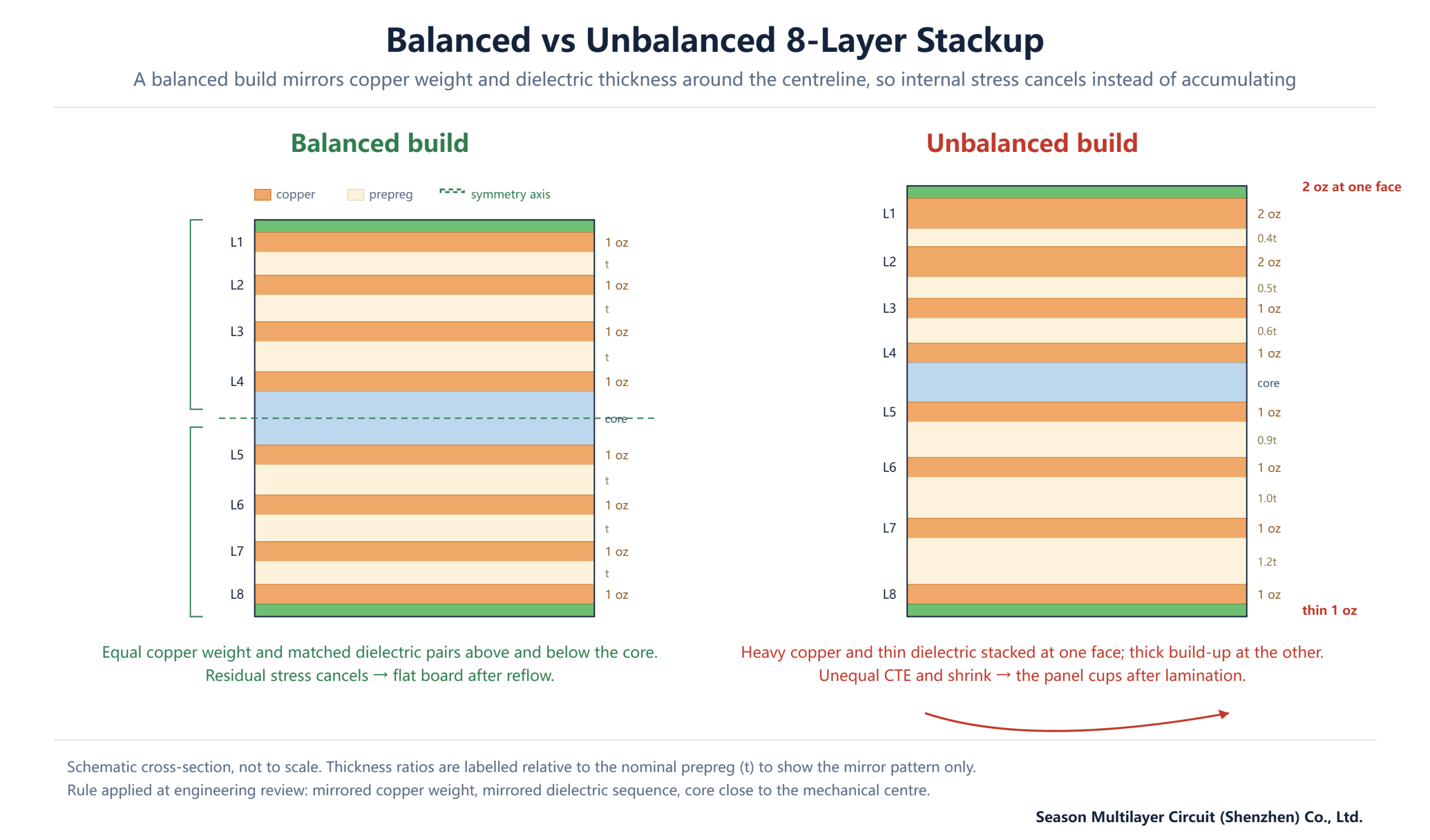
The term is easy to misread. A stackup is not balanced in the sense of every layer being identical — it is balanced in the sense that the distribution of copper and dielectric is symmetrical on either side of the mechanical centre of the board. Copper, epoxy resin and glass reinforcement each expand and shrink at different rates as the panel heats and cools, so only a mirrored distribution lets those movements cancel instead of adding up into a bending moment.
In practice, three properties need to be mirrored: copper weight, so 1 oz faces 1 oz and 2 oz faces 2 oz across the centreline; dielectric construction, so a thin prepreg pair near the top surface is matched by a thin pair near the bottom; and the position of the core, which should sit as close to the mid-plane as the layer count allows. A build that satisfies all three shrinks evenly during press and cools evenly after reflow.
Symmetry pays an electrical dividend as well. Mirrored ground planes give every signal layer a close, uninterrupted reference, which is why the same constructions that keep a board flat also hold impedance tolerance well. Lamination is where these stresses are locked in — the PCB lamination process article explains what the press does to the stack once it is closed.
Why Copper and Dielectric Symmetry Control Flatness
A rigid multilayer laminate is a composite of copper foil, cured epoxy and glass cloth. Each constituent has a different coefficient of thermal expansion and a different curing shrinkage. During the press cycle the resin melts, flows and cures; during cooling and any later reflow, the copper and the dielectric pull against each other. If the pull is equal above and below the neutral axis, the panel stays flat. If one face carries noticeably more copper — or a much stiffer dielectric sequence — the imbalance converts directly into curvature.
The failure shows up in two geometric forms. Bow is a cylindrical bend of the whole board, typically caused by layer-to-layer imbalance inside the build: a 2 oz plane pair on one side of the core against 1 oz signal layers on the other. Twist is a saddled deformation where two opposite corners lift out of plane, more often driven by panel-level asymmetry: heavy copper pours concentrated on one side of the panel, or uneven prepreg flow at the panel edge.
Both forms get worse as boards get thinner and larger. A 1.6 mm board hides small imbalances; a 1.0 mm board with the same asymmetry may exceed assembly limits before it ever reaches the oven. This is why a balanced PCB stackup is settled at design time — it cannot be inspected in afterwards.
Bow and Twist Limits to Design Against
Bow and twist are both expressed as a percentage: the maximum deviation from the reference plane, divided by the specified board length or diagonal, multiplied by one hundred. The figure below shows how the two differ geometrically and what typically causes each of them.
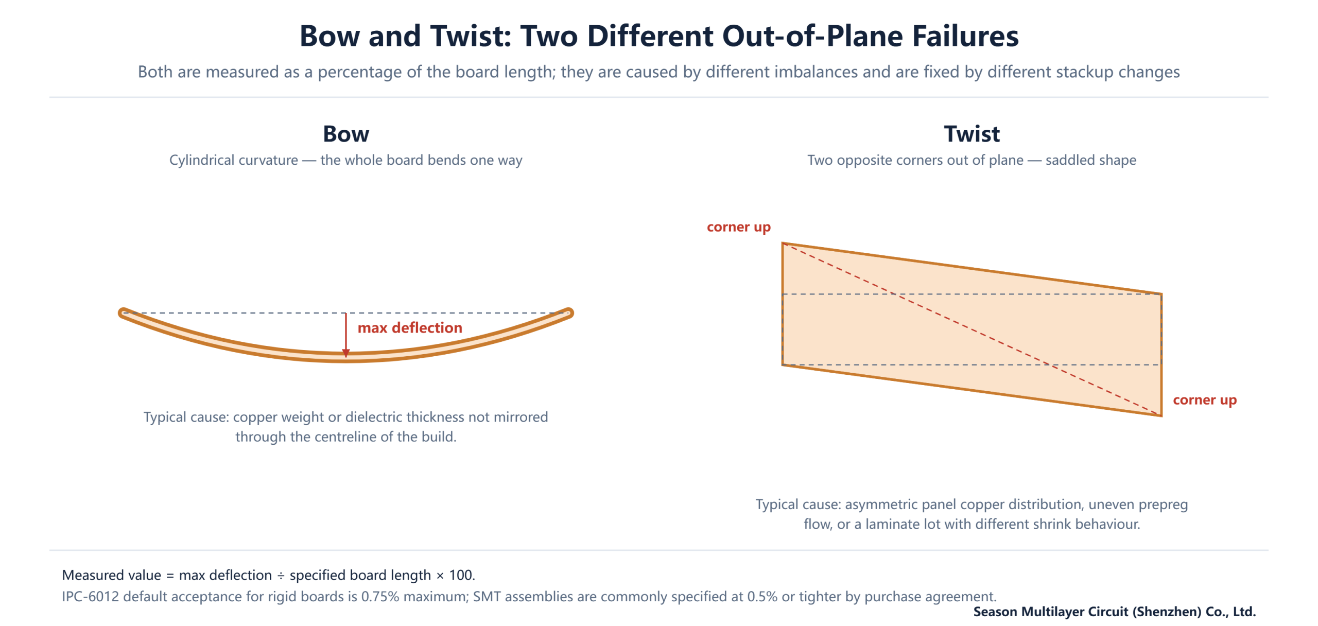
For acceptance, IPC-6012 sets a default maximum of 0.75% for rigid boards. Assemblies built with surface-mount components are commonly specified tighter — 0.5% or less — because fine-pitch BGAs and large connectors lose coplanarity well before a visually obvious warp appears. The number that matters for your build is the one written on the fabrication drawing, so decide it deliberately instead of inheriting the default.
A practical starting point: specify 0.75% for assemblies with through-hole and larger passive parts, and 0.5% whenever the board carries a BGA above roughly 0.8 mm pitch, a large QFN, or edge connectors. Panels destined for panelised SMT should be reviewed together with the breakout and carrier design, since twist at panel level is what the picker actually sees.
Copper Balance Rules for Multilayer Builds
Copper balance is more than matching plane copper weight layer by layer. The fabricator sees the copper distribution that survives etching, which includes signal routing, pours, and the dummy copper added to keep etch rates even. Four rules cover most designs:
- Mirror copper weight across the centreline — a 2 oz plane on L2 needs its counterpart on L7 in an 8-layer build, not a 1 oz signal layer.
- Pour copper on sparse signal layers so that finished copper coverage stays comparable between mirrored layer pairs; hatch or ground pours on routing layers do this job.
- Keep plane pairs symmetric: where a design needs two power planes, distribute them around the core rather than stacking both on one face.
- Flag heavy-copper layers (2 oz and above) in the stack table at quotation time, because they change both the press recipe and the symmetry plan.
Outer layers deserve special attention. Because outer copper is plated, its finished weight depends on routing density; a board with dense BGA fan-out on the top and mostly empty bottom needs dummy copper or thieving on the light side to keep the balanced PCB stackup intact. This is a normal request and far cheaper than re-spinning a warped panel — but it has to be visible in the Gerber, not described in an email.
Dielectric Symmetry and Prepreg Sequencing
The second half of symmetry lives in the dielectric. Prepreg sheets and cores differ in resin content and glass style, and each combination shrinks by its own amount during cure. A balanced PCB stackup therefore mirrors not just thickness but glass style: a 1080-style prepreg pair above the core is matched by the same style below it, and the two sub-cores of a 4-core build carry matched constructions.
Sequence matters as much as thickness. Two prepreg sheets of the same style can be stacked to reach a target dielectric height, but the resulting resin distribution differs from a single thicker sheet, and so does the flow behaviour around large plane windows. The fabricator picks the sequence; the designer’s job is to leave the dielectric targets as ranges rather than hard single values where possible, so symmetry and impedance can be satisfied simultaneously.
Laminate families also differ in curing behaviour, and the flammability and reliability requirements of the resin system are certified under UL rather than assumed. When a design mixes laminate lots or introduces a new material mid-project, re-check the symmetry plan — shrinkage behaviour is a property of the material, not only of the geometry.
Odd Layer Counts: How to Balance Them
An odd number of copper layers cannot be mirrored, which is why 5- and 7-layer builds are the classic warpage risk. The standard fix is to convert the construction into an even one by adding a layer that carries no signal: either a blank copper plane (electrically isolated, or tied to ground if the design allows) or an additional power plane. The added layer restores the mirror pair and usually improves power distribution at the same time.
The alternatives are less attractive. Splitting the odd layer into two thinner layers changes the layer count and the impedance plan; leaving the build odd and compensating with press parameters helps at the fabricator’s discretion but cannot remove the underlying asymmetry. Where the design genuinely cannot grow a layer, expect the engineering review to propose the least disruptive compensation and to verify flatness on the first article.
The simplest decision remains the best one: keep layer counts even unless there is a specific reason not to. If a routing study suggests five layers are enough, check whether the sixth layer as a ground plane improves return paths — in most digital designs it does, and the balanced PCB stackup comes for free.
Reference Stackups from 4 to 10 Layers
The tables below collect common constructions that hold a balanced PCB stackup together while staying manufacturable. They are starting points for a discussion, not universal answers — impedance targets, rail count and BGA fan-out all modify the final stack.
| Option | Build (top to bottom) | Strength | Watch-out |
|---|---|---|---|
| A — industry default | S1 – GND – PWR – S2 | Ground directly under S1; best reference for top-side critical signals | Keep the power-to-ground spacing thin, ideally no more than about 5 mil, to hold power-path impedance down |
| B — bottom-critical | S1 – PWR – GND – S2 | Gives the bottom layer the ground reference | Critical signals should then route on S2; top side loses its adjacent plane |
| C — shielded | PWR – S1 – GND – S2 | Surrounds S1 with planes on both sides for extra shielding | Only two routing layers; outer power plane complicates rework and test access |
For six layers and above, the pattern repeats: symmetric plane pairs around a central core, with the best routing layer adjacent to a ground plane on each side of the build.
| Layers | Reference build (top to bottom) | Notes |
|---|---|---|
| 6 | S1 – GND – S2 – PWR – S3 – S4 | Economy option when routing layers are tight; S2 is the preferred critical-signal layer |
| 6 | S1 – GND1 – S2 – PWR – GND2 – S3 | Industry default: two grounds flank the stack, S2 sits against GND1; keep the PWR-to-GND2 gap thin |
| 8 | S1 – GND1 – S2 – GND2 – PWR – S3 – GND3 – S4 | Default construction; S2 is the best routing layer, with grounds on both faces of the power distribution |
| 8 | S1 – GND1 – S2 – P1 – GND2 – S3 – P2 – S4 | For designs with several supply rails that one plane cannot serve; L3 and L6 become the best routing layers |
| 10 | S1 – GND1 – S2 – S3 – GND2 – PWR – S4 – S5 – GND3 – S6 | Single-rail default; four routing layers with adjacent references |
| 10 | S1 – GND1 – S2 – GND2 – P1 – P2 – GND3 – S3 – GND4 – S4 | EMC-driven dual-rail option; S2 and S3 are the optimum layers, and the two power planes can be separated to reduce inter-rail coupling |
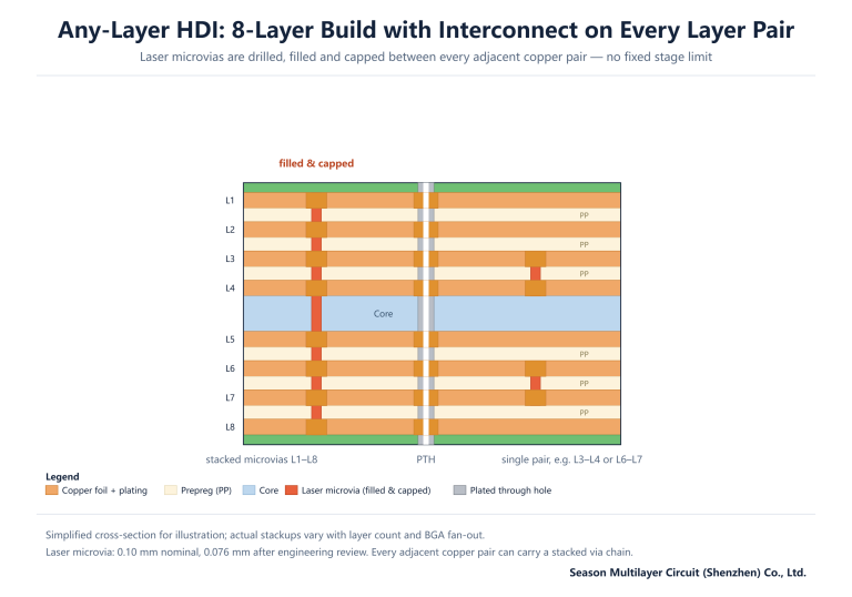
HDI constructions layer laser microvias on top of the same symmetric core logic — the HDI PCB technology guide shows how 1-Stage, 2-Stage and Any-layer builds extend these reference stacks without breaking the mirror.
How an Unbalanced PCB Stackup Fails in Assembly
Warpage rarely fails a bare board test — it fails downstream. The most common casualty is the large BGA: as the panel heats through reflow, an unbalanced build cups along its length, the package corners lift off the paste, and the result is open joints or bridges that only appear on boards that passed incoming inspection flat. The second casualty is the panelised process: twist that is tolerable on a single board ruins registration across a delivery panel, and the picker or printer drops parts at the panel edge.
Thickness compounds both effects. Thin builds — 1.0 mm and below — have less stiffness to resist the bending moment, so the same asymmetry produces more deflection than it would in a 1.6 mm board. Boards that combine thin construction with heavy outer copper, such as power stages in compact packages, are the highest-risk combination and deserve an explicit symmetry review.
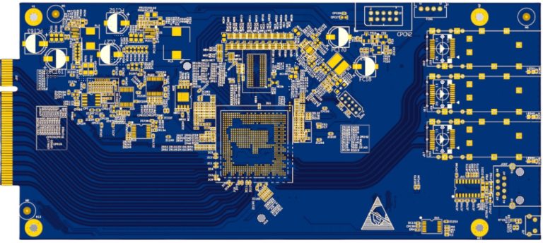
Both reference builds were planned as a balanced PCB stackup from the start — symmetric plane pairs and matched dielectric on both faces — which is what allows thin 8-layer and 10-layer constructions to run through reflow flat. See the 8-layer intelligent terminal PCB and the 10-layer 2-Stage HDI prototype for the finished constructions.
A Stackup Balance Checklist Before Release
Most warpage problems are visible in the stack table before any Gerber is plotted. Run this check before releasing a new multilayer design, and again whenever layer count, copper weight or material changes:
| Check | What to verify | Why it matters |
|---|---|---|
| Layer count parity | Even number of copper layers, or a documented compensation plan | Odd counts cannot be mirrored and are the top warpage risk |
| Copper mirror | 1 oz faces 1 oz, 2 oz faces 2 oz across the centreline, including pours and thieving | Copper imbalance converts directly into bow |
| Dielectric mirror | Matched prepreg style and thickness above and below the core | Resin shrinkage imbalance converts into bow and twist |
| Core position | Core sits at or near the mechanical mid-plane of the build | The neutral axis is where stresses must cancel |
| Plane pair symmetry | Power and ground planes distributed around the centre, not stacked on one face | Stacked planes concentrate stiffness on one side |
| Drawing limit | Bow and twist limit written on the fabrication drawing (0.75% default, 0.5% for fine-pitch SMT) | Acceptance is only as tight as the number on the drawing |
If any line of this table is unresolved, resolve it before tooling so the balanced PCB stackup reaches the press intact. Our multilayer PCB manufacturing capability page lists the layer counts and copper weights this review covers, and the manufacturer selection checklist explains how to compare fabricators on stackup engineering alone.
Frequently Asked Questions
What makes a PCB stackup balanced?
A balanced PCB stackup mirrors copper weight, prepreg construction and the position of the core around the mechanical centre of the board. Each mirrored pair — copper layer against copper layer, dielectric against dielectric — produces equal and opposite stress during lamination and reflow, so the panel stays flat instead of bowing or twisting.
Does an odd layer count always warp the board?
Not always, but it removes the possibility of a perfect mirror, which is why 5- and 7-layer builds carry higher warpage risk. The usual fix is adding a blank copper or power layer to make the count even and restore symmetry. If the layer count cannot change, the fabricator compensates with press parameters and verifies flatness on the first article.
What bow and twist limit should I specify for SMT assembly?
IPC-6012 defaults to 0.75% maximum for rigid boards. For assemblies with fine-pitch BGAs, large QFN packages or edge connectors, 0.5% or tighter is commonly specified by agreement. Write the limit on the fabrication drawing so incoming inspection and the assembly line measure against the same number.
How does copper balancing affect the cost of a multilayer board?
Balance is mostly a design-side activity: pouring copper on sparse layers and mirroring plane pairs costs essentially nothing extra in material. It becomes a cost item when the imbalance is discovered late — re-spinning a warped panel costs far more than adding dummy copper in the original Gerber, which is why the review happens at quotation.
Can I keep a stackup balanced and still hit tight impedance targets?
Yes, and the two goals usually agree. Symmetric ground planes give every routing layer a close reference, which stabilises impedance. The workflow is to fix the symmetric dielectric pairs first, then tune trace widths and heights within those pairs. If a target conflicts with the mirror, flag it at engineering review rather than breaking symmetry silently.
Should the core always sit in the middle of the stackup?
For most multilayer builds, yes — the core is the stiffest, most dimensionally stable element, so placing it on the neutral axis lets the softer prepreg layers mirror around it. Some HDI and backplane constructions deliberately deviate for impedance or thickness reasons, but the deviation should be a reviewed decision with the flatness risk stated, not an accident of the stack table.
What information does the fabricator need to review stackup balance?
Send the layer stack table with copper weights and dielectric targets, the Gerber set so actual copper distribution can be measured, impedance targets per class, and the assembly context — thinnest board area, largest BGA, panelisation plan. With those four items, a symmetry review takes a single engineering pass and usually settles the construction in one round.
Get Your Balanced PCB Stackup Reviewed Before Tooling
Send your layer stack table and Gerber set, and our engineering team will return a symmetry review — copper mirror, dielectric sequencing, bow and twist limits, and a proposed construction — before the panel is tooled. Start from the PCB manufacturing services overview or submit your files for a stackup and impedance review directly.