Skip to content
Home
Services
Products
Fast PCB
Multilayer PCB
HDI PCB
High Speed PCB
High Frequency PCB
Rigid-Flex PCB
PCBA
Instant PCB Quote
About Us
Company Profile
Factory Display
Process Capability
Lead Time
HDI PCB Technology
PCB Materials and Laminates
News
Contact
Book Appointment Now
(+86) 18681528532
24/7 Emergency Phone
Home
Services
Products
Fast PCB
Multilayer PCB
HDI PCB
High Speed PCB
High Frequency PCB
Rigid-Flex PCB
PCBA
Instant PCB Quote
About Us
Company Profile
Factory Display
Process Capability
Lead Time
HDI PCB Technology
PCB Materials and Laminates
News
Contact
(+86) 18681528532
24/7 Emergency Phone
Menu
PCB Basics
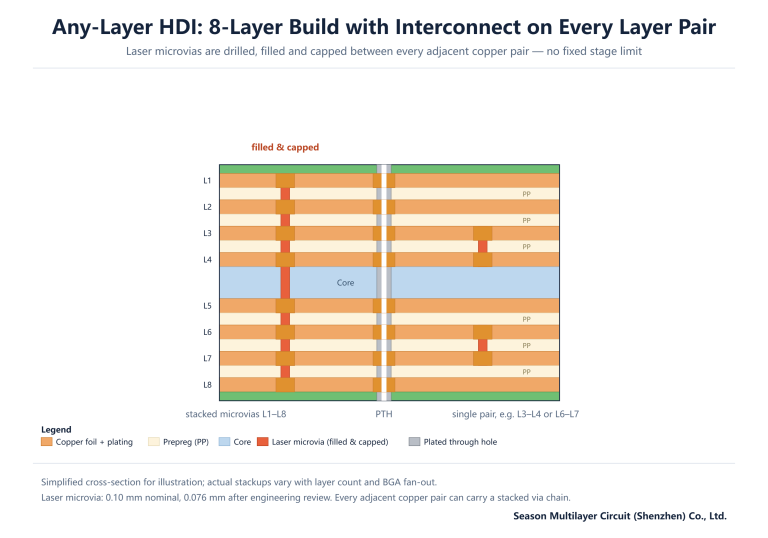
Any-Layer HDI Explained: ELIC Stackup, Process Flow and When to Use It
What Is a High-Speed PCB? Design Rules, Stackup and Manufacturing Limits
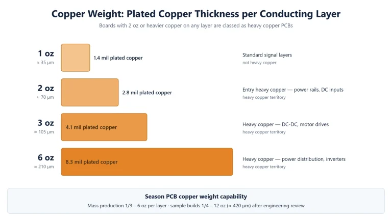
Heavy Copper PCB: Copper Weight, Current Capacity and When to Spec It
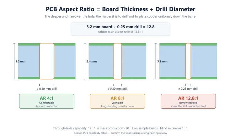
PCB Aspect Ratio Explained: Hole Size, Plating Throw and Design Limits
PCB Inner Layer Fabrication: Dry Film, Etching and AOI
PCB Panel Cutting Explained: Unit, Set and Panel Sizing Basics
High-Frequency PCB: Materials, Dk/Df and When to Spec Them
PCB Lamination Process: How Multilayer Boards Are Pressed and Bonded
PCB Drilling Process: Mechanical vs Laser Drilling Explained
How to Choose a Multilayer PCB Manufacturer: A 5-Step Checklist
PCB Impedance Measurement Methods: TDR, VNA, Flying Probe and Coupons
Electroless Copper Deposition in PCB: How the PTH Process Works
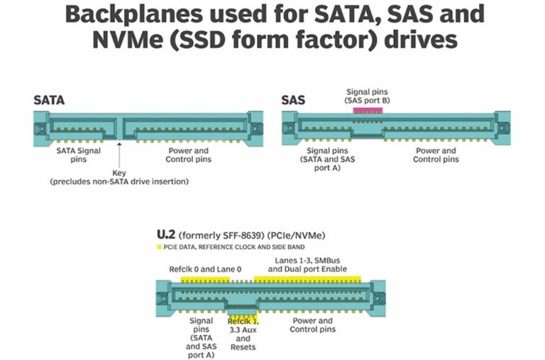
U.2 SSD PCB Design: SFF-8639 Carrier Board Layout and Build Rules
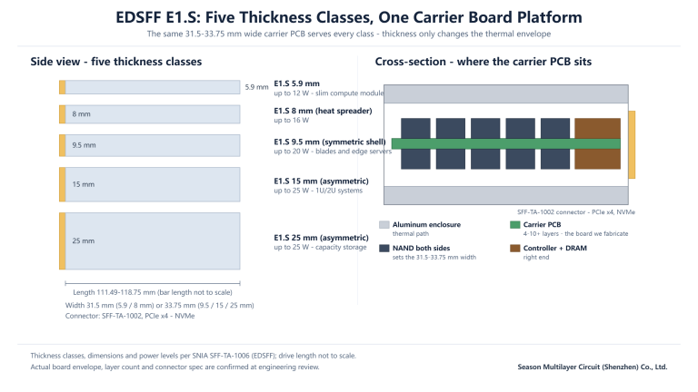
E1.S SSD PCB Design: EDSFF Carrier Board Stackup and Fabrication Rules
Via-in-Pad Technology for HDI and BGA Boards: Process and Rules
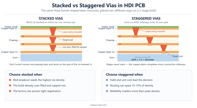
Stacked vs Staggered Vias in HDI PCB: Structures, Cost and Yield
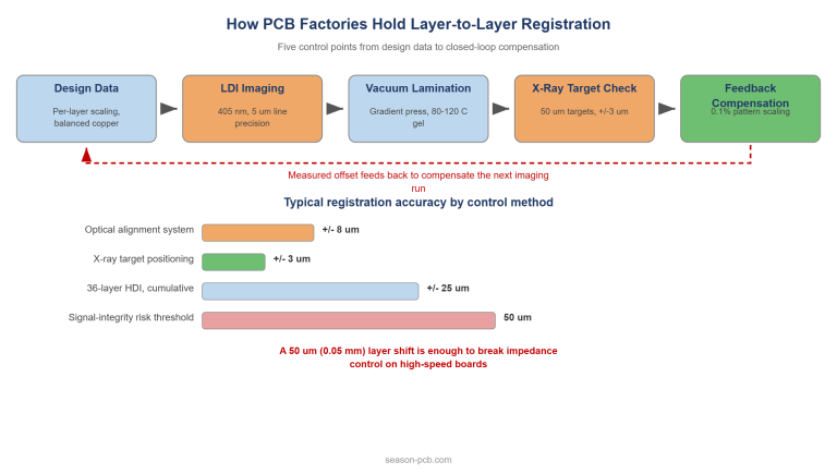
PCB Layer-to-Layer Registration Tolerance: How Factories Hold ±25 µm
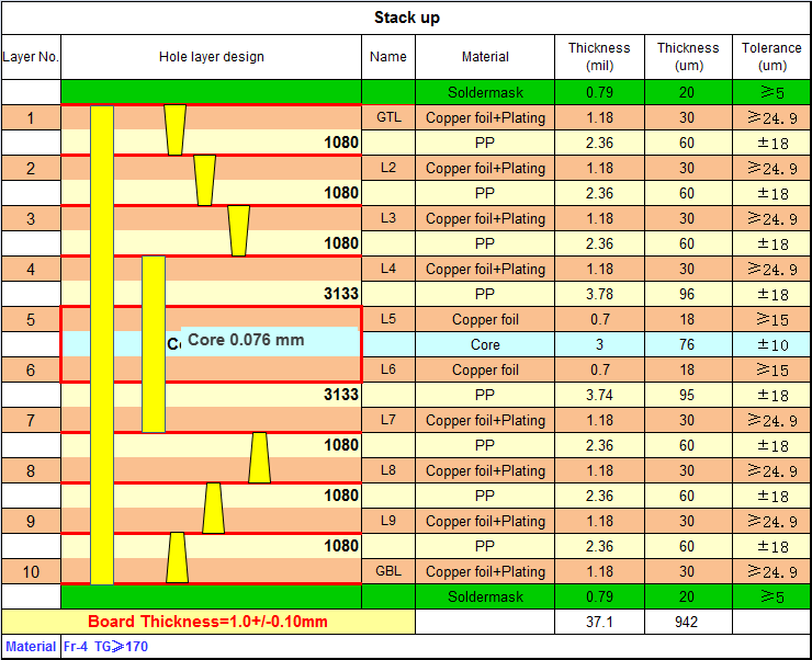
10-Layer 3-Stage HDI Stackup: Standard and Simplified Builds
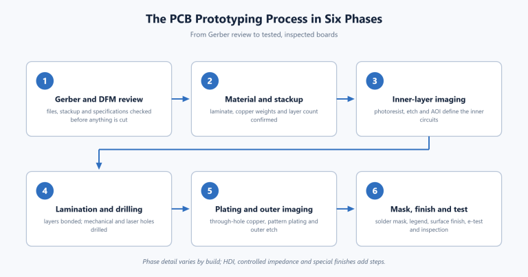
PCB Prototyping Process: From Gerber Files to First Article
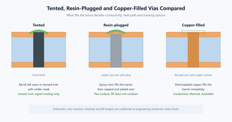
Copper Filled Vias: Via Filling Plating Process and Design Rules
1
2
3
Next