Book Appointment Now

PCB impedance measurement methods compared: TDR, VNA and SWR, flying probe, LCR meters and test coupons, with trade-offs and factory control.
PCB Impedance Measurement Methods: TDR, VNA, Flying Probe and Coupons
When a stackup calls for 50 Ω single-ended or 100 Ω differential pairs, the number on the drawing is a promise someone has to verify in copper. Simulation gets you close, laminate tolerances get you in the neighborhood — but only a physical PCB impedance measurement on real production panels tells you whether the board in front of you will transmit signals cleanly or reflect half of them back at the driver.
This guide explains the five methods actually used in PCB manufacturing and incoming inspection — time-domain reflectometry (TDR), vector network analyzer / SWR testing, flying probe, LCR meters and the impedance test coupon — how each one works, where it is strong, and where its readings mislead. It closes with the practical factors that skew results and how a factory turns a nominal impedance into a controlled, documented process.
Table of Contents
- Why Controlled Impedance Must Be Measured, Not Assumed
- What PCB Impedance Measurement Actually Checks
- TDR: How Time-Domain Reflectometry Measures a Trace
- VNA and SWR Testing for RF Structures
- Flying Probe Testing on Bare Boards
- Impedance Test Coupons: The Evidence That Ships With the Board
- Where LCR Meters Fit — and Where They Do Not
- Choosing Among the Five PCB Impedance Measurement Methods
- Five Factors That Skew Impedance Test Results
- How a Factory Turns an Impedance Target Into Production Control
- FAQ
- Get Your Stackup and Impedance Windows Reviewed
Why Controlled Impedance Must Be Measured, Not Assumed
Characteristic impedance is the ratio of voltage to current as a signal propagates down a transmission line — a property of the trace geometry, the dielectric around it, and the reference planes. It combines resistance, inductance and capacitance effects, and at high edge rates it dominates signal behavior long before DC resistance matters.
The problem for production is tolerance stacking. Copper thickness, etch compensation, prepreg thickness and dielectric constant all vary within industry-normal ranges. A stackup simulated at exactly 100 Ω can easily land at 106 Ω on the shop floor if nobody closes the loop with a measurement. That mismatch shows up as reflections, ringing, undershoot and failed compliance testing at the system level — faults that are miserable to debug on an assembled board.
Typical design targets and the tolerances a controlled-impedance order commits to are summarized below. Tighter windows are achievable, but each step down narrows the process window in etch, lamination and material selection, so they should be specified only where the interface standard actually requires them.
| Target | Typical Application | Commonly Committed Tolerance |
|---|---|---|
| 50 Ω single-ended | General high-speed digital, RF lines | ±10% |
| 90 Ω differential | USB, DDR routing groups | ±8% |
| 100 Ω differential | Ethernet, PCIe-class differential pairs | ±8% |
| Critical RF / matched structures | Tight-match RF and antenna feeds | ±5% on engineering review |
What PCB Impedance Measurement Actually Checks
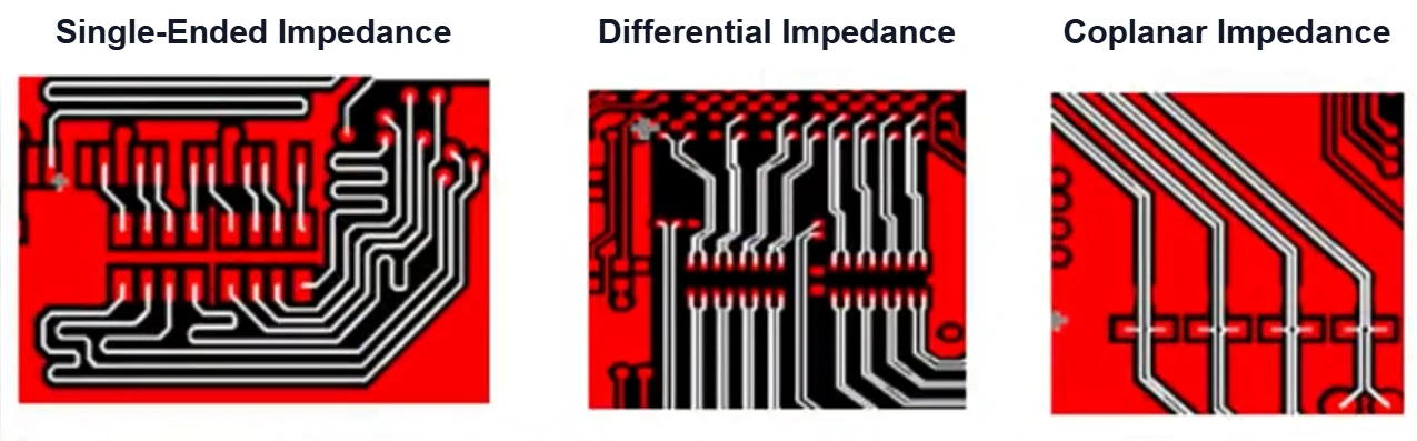
On artwork, impedance control applies to three main structures. Single-ended impedance describes one signal trace against its reference plane. Differential impedance describes a pair routed together, where the coupling between the two legs lowers the effective impedance below that of either leg alone. Coplanar structures add ground shapes alongside the trace on the same layer, changing the field distribution again.
A measurement campaign answers a deceptively simple question: for every controlled structure in the design, does the manufactured board fall inside the committed tolerance window? Answering it requires matching the method to the structure — a bare-board coupon measurement, a driven differential pair on a finished board, and an RF feedline evaluated over frequency each behave differently, which is why production floors keep more than one instrument class available.
TDR: How Time-Domain Reflectometry Measures a Trace
TDR is the workhorse of bare-board production testing. The instrument — output impedance 50 Ω — launches a fast step edge into the trace under test through a matched cable. Wherever the transmission environment changes impedance, part of the edge reflects back; the instrument samples that reflection and compares it with the reflection produced by a known standard, converting the amplitude difference into an impedance profile along the line.
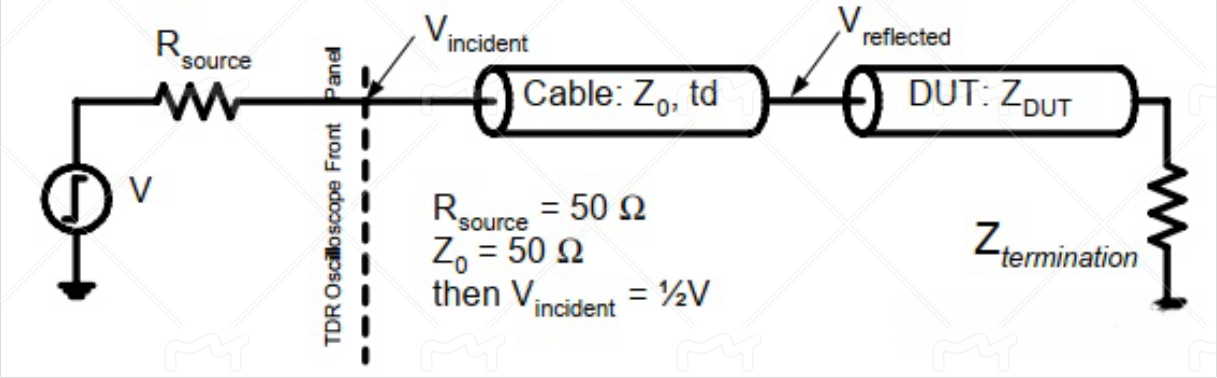
The strength of the method is localization: it shows not just that a board deviates, but where — an open, a short, a neck-down at a BGA breakout, or a uniform shift across every trace. That makes it equally useful for factory process control and for failure analysis on a suspect design.
Its limits are worth respecting. Absolute accuracy on a specific trace depends on calibration quality, probe contact parasitics and the launch region of the measurement; readings in the first centimeter after the probe are contaminated by the launch transition. For production ±8–10% windows this rarely matters, but chasing ±5% numbers on short features demands careful setup and a quiet electrical environment.
VNA and SWR Testing for RF Structures
Where TDR works in the time domain, a vector network analyzer works in the frequency domain. The VNA injects a continuous wave at a known frequency and measures the relationship between the incident and reflected waves, from which standing wave ratio (SWR) and return loss follow. A perfectly matched line reads SWR 1; any mismatch pushes the ratio above 1, with worse matches reading higher.
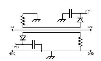
For RF and high-frequency analog work this is the more natural view: what matters is behavior across the operating band, not the location of one discontinuity. Sweeping SWR across frequency reveals how an antenna feed, filter or connector transition behaves under real operating conditions — information a single TDR number cannot provide.
The trade-offs mirror the strengths: VNA-class instruments are a significant investment, and meaningful results demand calibrated, repeatable fixturing and a skilled operator. In practice, RF-grade verification lives with design labs and specialist test houses more than on the assembly line, which is exactly why the humble test coupon carries so much weight in production — it lets a factory verify what the RF team will later confirm in the band.
Flying Probe Testing on Bare Boards
Flying probe systems mount programmable pins on robotic arms that touch down directly on test points, measuring continuity, isolation and — on machines equipped for it — impedance on nets without any dedicated fixture. For prototypes and low-volume production, that flexibility is decisive: the program follows the netlist, so a design revision costs a software change rather than new tooling.
As an impedance method it has natural limits. Contact repeatability at the probe tip and the geometry of reaching fine-pitch structures constrain absolute accuracy, and throughput is far below a fixtured solution. The pragmatic role is clear: flying probe is excellent for catching gross defects and verifying prototype builds quickly, while the impedance data of record for volume shipments comes from coupons measured on calibrated bench instruments.
Impedance Test Coupons: The Evidence That Ships With the Board
A test coupon is a small strip of circuitry built on the production panel itself, replicating the controlled structures — same stackup, same materials, same etch batch — in a form that is easy to measure. Because it travels through every process step with the real boards, its measured impedance is direct evidence about the panel, not a simulation.
Coupons are usually placed in the panel frame and removed after fabrication. The factory measures them on a TDR bench, records the values against the order specification, and ships the results with the paperwork on request. For designers, two details matter: the coupon must replicate the actual trace geometry including reference plane distances, and it represents the panel statistically — it cannot prove every trace on every board, but it is the industry-standard sampling method and the basis on which impedance orders are accepted.
One practical habit: on controlled-impedance revisions, ask whether the coupon design was updated when the stackup changed. A stale coupon that no longer mirrors the production structures is one of the quiet ways an impedance claim stops meaning anything.
Where LCR Meters Fit — and Where They Do Not
LCR meters measure inductance, capacitance and resistance precisely on components, and with careful fixturing they can extract partial impedance data from simple structures. For a design-stage sanity check — estimating what a trace geometry implies before committing a stackup — they are a low-cost first look.
As a production acceptance method for controlled transmission lines they are simply the wrong tool: a transmission line’s characteristic impedance is a traveling-wave property that a lumped-element measurement at low frequency does not reproduce. Treat LCR readings as indicative modeling aids, never as evidence that a 100 Ω pair landed on target.
Choosing Among the Five PCB Impedance Measurement Methods
The five methods are complements, not competitors — each answers a different question at a different stage. The comparison below condenses the trade-offs into the form a hardware PM needs when reviewing a supplier’s test plan.
| Method | What It Delivers | Best Used For | Main Limits |
|---|---|---|---|
| TDR | Impedance profile along a trace; locates discontinuities | Bare-board production testing and failure analysis | Launch-region contamination; needs controlled setup |
| VNA / SWR | Match quality across frequency (SWR, return loss) | RF feedlines, antennas, band-limited structures | Instrument cost; calibration and operator skill |
| Flying probe | Fixtureless continuity, isolation and basic impedance | Prototypes and low-volume runs, fast revisions | Contact repeatability; low throughput |
| LCR meter | Lumped L/C/R estimates | Early design estimates on simple structures | Not valid for transmission-line acceptance |
| Test coupon | Documented impedance of record for the panel | Volume orders, shipping evidence, audits | Sampling — represents the panel, not every trace |
A sound supplier test plan combines them in layers: coupon measurements per panel as the baseline evidence, TDR profiling when something drifts or a failure needs localization, and RF-band verification reserved for designs whose interfaces genuinely demand it. Anything less starts to look like impedance control by paperwork.
Five Factors That Skew Impedance Test Results
Between a correct stackup and a trustworthy number sits the measurement itself, and five factors routinely move results. Environment comes first: temperature and humidity affect both instrument drift and the dielectric response of the board, so stable conditions beat heroic correction factors.
Second, instrument selection and calibration — a 50 Ω reference that is actually 49.2 Ω shifts every reading. Third, parameter setup: the step rate or test frequency must reflect the application, since fast digital interfaces behave differently from the slow edges a casual setup exercises. Fourth, test-point selection: probing near a discontinuity or launch transition measures the fixture as much as the board.
Fifth, and most underrated, is data discipline. Results only become process control when they are recorded against panel IDs, compared against the committed tolerance, and fed back into etch compensation and lamination settings. A measurement that is not archived cannot be trended — and impedance problems announce themselves as trends before they appear as escapes.
How a Factory Turns an Impedance Target Into Production Control
On the manufacturing side, the flow starts before any panel exists. Stackup engineering converts the requested impedance into trace widths, spacings and dielectric choices using the field solver, calibrated against the measured Dk of the actual laminate lots in stock — which is why material selection and impedance control are inseparable, as covered in our PCB materials and laminates guide.
During fabrication, coupon measurements close the loop per panel: values inside tolerance ship, values drifting toward the window edge trigger etch-compensation adjustments for the next panel. Designs that mix dielectrics add another verification layer, described in our hybrid stackup guide, while high-speed multilayer work such as our automotive high-speed backplane and 10-layer 2-stage HDI prototype platforms runs this control across dense differential groups.
For RF and microwave boards the same discipline extends to low-loss laminates — our double-sided high-frequency PCB line is a typical example — where the dielectric lot, copper roughness and etch quality all influence the final measured impedance. The acceptance criteria should reference recognized IPC design and acceptance standards so both sides measure the same thing the same way.
Frequently Asked Questions
What is PCB impedance measurement?
It is the set of methods used to verify that manufactured traces hit their designed characteristic impedance — typically 50 Ω single-ended or 90–100 Ω differential. Production relies mainly on TDR profiling and impedance test coupons, with VNA/SWR methods reserved for RF structures that need verification across frequency.
How does a TDR impedance test work?
The instrument launches a fast step edge with a 50 Ω source impedance into the trace through a matched cable. Any impedance change along the path reflects part of the edge; sampling and comparing that reflection against a known standard yields an impedance profile along the line, including the location and size of opens, shorts and mismatched sections.
What tolerance can be committed on controlled impedance?
Commonly ±10% for standard single-ended lines and ±8% for differential pairs such as 90 Ω USB or 100 Ω Ethernet structures. Tighter windows, down to about ±5%, are achievable but narrow the etch and lamination process window, so they should be requested only where the interface standard genuinely requires them and confirmed at engineering review.
What is an impedance test coupon?
A small strip of test structures built on the production panel itself, replicating the controlled traces, stackup and materials. Because it passes through every process step with the real boards, measuring it on a calibrated TDR bench provides documented, panel-specific evidence that the order met its impedance specification.
Why is SWR testing used instead of TDR for some boards?
RF structures are judged by how well they stay matched across the operating band, not by the location of a single discontinuity. A VNA-based SWR sweep shows match quality at every frequency of interest, which is the natural acceptance view for antenna feeds and RF front ends, while TDR answers time-domain questions such as where a discontinuity sits.
Can an LCR meter verify controlled impedance?
No, not for acceptance. LCR meters measure lumped inductance, capacitance and resistance, while characteristic impedance is a traveling-wave property of a transmission line. They are useful for early design estimates on simple structures, but shipping evidence must come from TDR or coupon measurements made for that purpose.
Does every impedance-controlled design need a test coupon?
In volume production, effectively yes — the coupon is the industry-standard sampling method and the basis on which impedance orders are accepted and audited. For prototypes it is equally valuable, and any stackup revision should regenerate the coupon so the measured structures keep mirroring the real traces.
Get Your Stackup and Impedance Windows Reviewed
Send your Gerber data, stackup draft and impedance table — targets, tolerances and the interfaces behind them — for an engineering review before fabrication. Our team will confirm which structures are measurable on coupons, whether the committed windows match current process capability, and where a small design change buys real margin. Submit through the quote request page and you will receive a manufacturability response with lead time confirmed at engineering review, backed by documented production capability.