Book Appointment Now

PCB aspect ratio decides whether your vias can be drilled and plated reliably. Learn how to calculate it, where the real limits sit, and how to design around them.
PCB Aspect Ratio Explained: Hole Size, Plating Throw and Design Limits
A via that looks fine in your CAD file can come back from the factory with thin copper in the middle of its barrel, or be rejected before production even starts. In most cases the cause is one number nobody checked: the PCB aspect ratio — finished board thickness divided by finished hole diameter. This guide explains how the ratio is calculated, why it controls both drilling and plating quality, where the real limits sit today, and which design levers bring a marginal stackup back into safe territory. Every limit quoted here comes from our published process capability table — through-holes at 12:1 in mass production and 20:1 on sample builds, blind microvias at 1:1 — the same limits our CAM engineers apply when they review incoming Gerber data. If you want the full parameter sheet while you read, it is maintained on our PCB manufacturing capability page.
Table of Contents
- What Is PCB Aspect Ratio and How Do You Calculate It
- PCB Aspect Ratio Limits Today: 12:1 Production, 20:1 Sample
- Why High Aspect Ratio Holes Are Hard to Plate
- Drilling Depth, Wander and Hole Quality
- PCB Aspect Ratio and Signal Integrity
- Mechanical and Reliability Effects of Deep, Narrow Holes
- How to Reduce Aspect Ratio Without Redesigning the Product
- What to Put in Your Fabrication Notes
- Cost and Lead Time Implications
- FAQ
- Have Your Stackup Checked Before You Order
What Is PCB Aspect Ratio and How Do You Calculate It
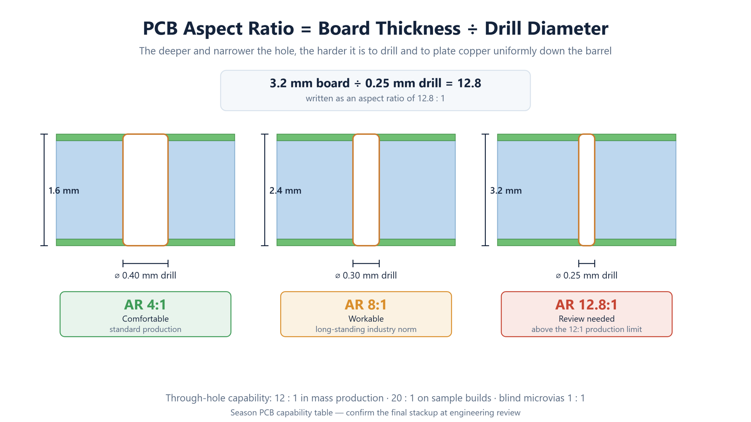
The PCB aspect ratio is the depth of a hole relative to its diameter. For a through-hole it is simply finished board thickness divided by finished hole diameter: a 1.6 mm board drilled with 0.4 mm holes sits at 4:1, while a 3.2 mm backplane drilled with 0.25 mm tools reaches 12.8:1. The same arithmetic applies to any vertical interconnect, which is why the ratio is one of the first numbers a fabricator checks on a new stackup.
A classic worked example from the industry: a 100 mil (2.54 mm) thick board with 10 mil (0.25 mm) holes has a 10:1 ratio. Every step deeper, or every tenth of a millimetre narrower, makes the hole harder to drill cleanly and harder to plate with uniform copper. The table below shows how quickly the verdict changes as the number climbs.
| Board thickness | Drill diameter | Aspect ratio | Typical verdict |
|---|---|---|---|
| 1.6 mm | 0.40 mm | 4:1 | Comfortable — standard production |
| 2.4 mm | 0.30 mm | 8:1 | Workable — long-standing industry norm |
| 3.2 mm | 0.25 mm | 12.8:1 | Above the 12:1 production limit — needs review or sample build |
One wording trap worth avoiding: drill diameter and finished hole diameter are not the same number. Electroplating grows the barrel by the plated copper thickness on each wall, so a 0.25 mm drill typically produces a slightly larger finished hole. Quotes and fab notes should state which figure the ratio was calculated from, because a 0.05 mm difference can move a design across a limit.
PCB Aspect Ratio Limits Today: 12:1 Production, 20:1 Sample
For years the rule of thumb was 8:1. Spindle technology, drill bit materials, desmear chemistry and plating baths have all improved since, and modern factories now push further. Our own numbers are 12:1 for through-holes in volume production and 20:1 on sample builds, where feasibility is confirmed lot by lot after engineering review. Blind microvias follow a separate rule — 1:1 in production, 1.2:1 on samples — because a laser-drilled blind hole plates from one side only.
| Parameter | Mass production | Sample |
|---|---|---|
| Layer count | 2–30 | 2–64 |
| Finished board thickness | 0.2–6.0 mm | 0.15–20 mm |
| Minimum mechanical drill | 0.15 mm (6 mil) | 0.127 mm (5 mil) |
| Minimum microvia | 0.10 mm (4 mil) | 0.076 mm (3 mil) |
| Through-hole aspect ratio | 12:1 | 20:1 |
| Blind via aspect ratio | 1:1 | 1.2:1 |
The gap between the two columns matters when you plan a product ramp. A 16:1 hole may prototype successfully on a sample build, then fail at quotation for mass production. If your board lives near the limit, ask early which column it falls into — and remember that plating uniformity, not drilling, is usually the binding constraint as the table in the next section explains.
Why High Aspect Ratio Holes Are Hard to Plate
Every through-hole must be copper-plated along its entire barrel so the top and bottom layers are connected with low resistance. Electrically, the plating current prefers short, open paths: it concentrates near the hole entrances and weakens with depth. The deeper and narrower the hole, the less current reaches the middle of the barrel — a behaviour called plating throw. At 4:1 the difference barely matters; at 12:1 the mid-barrel can plate significantly thinner than the ends unless the process compensates.
Factories fight this with chemistry and electrical engineering: electroless copper first lays a conductive seed uniformly on the resin and glass of the bore, then acid copper plating builds thickness with modified bath chemistry, tailored current waveforms and strong solution agitation through the hole. The process is described step by step in our electroless copper deposition guide.
The consequence for designers is simple: a high hole aspect ratio costs margin. If the mid-barrel plates to 15 µm where the ends reach 25 µm, the via carries less current and is more fragile during assembly. Reputable fabricators therefore check the expected ratio at CAM and either adjust the plating recipe, propose a design change, or quote the board into their sample capability column instead of production.
Drilling Depth, Wander and Hole Quality
Before plating comes the hole itself, and a high PCB aspect ratio is just as demanding here. A 0.20 mm drill plunging 4 mm into a stack behaves differently from the same tool in a 1.6 mm panel: the longer unsupported length flexes, deflects against glass fibre bundles, and generates more heat. Push deep enough and the bit wanders, the hole goes off-centre against inner-layer pads, or smearing seals the barrel so plating chemistry cannot reach the wall.
Hole quality at depth is managed with peck drilling cycles, reduced in-feed rates, fresh tool changes and strict hit counts per drill, all of which consume machine time. Depth-to-diameter also interacts with layer registration: the deeper the hole, the more accumulated layer-to-layer misalignment shows up at its ends. Our drilling overview explains how mechanical and laser drilling lines split this work between standard through-holes and microvias.
- Bit deflection and wander rise with unsupported drill length
- Smear and debris must be cleared by desmear before plating
- Entry and exit burrs grow with dwell time at depth
- Tool changes are scheduled more often on high-ratio panels
- Registration tolerance compounds over the full stack depth
None of these effects is exotic — they are routine at any multilayer shop. What changes with ratio is how much process margin each one consumes, which is why the same design can be routine at one factory and borderline at another. Our PCB drilling process guide covers the equipment side in detail.
PCB Aspect Ratio and Signal Integrity
On thick, high-layer-count boards the aspect ratio has an electrical signature too. A through-hole that spans a 3.2 mm stack leaves a long unused barrel — a stub — below the layer where the signal actually exits. Long stubs resonate at frequencies that matter for multi-gigabit links, and the effect grows directly with board thickness. This is one reason backplane and server boards pay close attention to hole geometry long before fabrication starts.
The standard countermeasure is controlled-depth drilling: a second drill pass removes most of the unused barrel after plating, shortening the stub. We run controlled-depth back drilling as a standard special process, and it pairs naturally with thick backplane builds — our 12-layer automotive high-speed backplane PCB is a typical home for the technique. TDR-based verification then closes the loop between the stackup proposal and the finished panel, as described in our impedance measurement guide.
For most designs below roughly 1.6 mm thickness the electrical effect of hole depth is negligible and does not justify extra process steps. The pattern to remember: aspect ratio drives stub length, stub length drives resonances, and resonances are cheap to avoid at design time and expensive to fix after panels are built.
Mechanical and Reliability Effects of Deep, Narrow Holes
The plated barrel is the structural spine of a via, and it lives under constant mechanical stress. Copper inside the hole expands and contracts at a different rate than the surrounding laminate, so every assembly reflow and every field temperature swing flexes the barrel. A well-plated 8:1 hole absorbs this for thousands of cycles; a 14:1 hole with a thin mid-barrel has far less copper cross-section to work with, and that is where cracks prefer to start.
Acceptance criteria make the difference explicit. Production boards are inspected to IPC Class 2 by default, with Class 3 acceptance available for high-reliability programmes — the IPC standards family defines how barrel thickness and hole quality are judged. On vibration-prone products such as vehicle electronics and factory equipment, we recommend confirming the plating uniformity expectation at engineering review rather than discovering it in microsection after the first lot.
Board thickness also plays a mechanical role of its own: thicker boards are stiffer in bending but concentrate more stress at rigid interfaces such as edge connectors and large BGA fields. High hole aspect ratio and high board mass tend to arrive together, so reliability review should look at both — the holes and the board they live in.
How to Reduce Aspect Ratio Without Redesigning the Product
When a stackup lands above the production limit, the fix is rarely a full redesign. Most boards can be brought back inside the ratio by attacking one of its two factors — thickness or hole size — and usually with changes that cost far less than the scrap risk they remove. Work through the levers in this order, which mirrors how our CAM engineers typically sequence suggestions.
- Widen the smallest drills where the current and pad geometry allow it — the cheapest lever available
- Move high-current paths onto planes and replace parallel narrow traces with more, larger vias
- Split an over-thick board into two thinner boards joined at a connector or board-to-board interface
- Shift dense breakout regions onto blind and buried vias so the through-holes carry less traffic
- Choose a higher layer count on thinner cores to reach the same function in a shorter stack
- Specify buried via structures for inner-layer switching so outer layers keep generous hole sizes
Each lever has a cost side: more lamination cycles for buried-via structures, more layers for thin-core stacks, connector outlay for split boards. The right answer depends on volume, and the arithmetic is straightforward to compare — which is exactly what a stackup review is for. Bring the aspect ratio question to the fabricator while the layout is still plastic, and one of these levers almost always resolves the margin problem.
What to Put in Your Fabrication Notes
Clear fab notes prevent the most common aspect-ratio misunderstanding: two companies calculating from different numbers. State the finished thickness, the minimum hole, and which figure your ratio was computed from. The wording examples below take a minute to add to a drawing and remove an entire round of quotation back-and-forth.
| Fab note item | Example wording |
|---|---|
| Finished board thickness | 2.4 mm finished, ±10% |
| Minimum finished hole | 0.30 mm |
| Aspect ratio intent | Prefer 8:1 or lower; accept up to 10:1 after review |
| Acceptance class | IPC-A-600 Class 2, Class 3 on request |
| Microvia structures | 1+N+1 blind via, 0.10 mm finished |
If your drawing already carries these lines, a fabricator can quote the board against its real capability columns instead of guessing. If it does not, expect the question to come back anyway — better from a CAM engineer before order confirmation than from a microsection report after delivery. Our copper-filled via guide covers the related plugging and filling callouts that often share the same drawing.
Cost and Lead Time Implications
Aspect ratio drives cost through process time, not through exotic materials. A high-ratio panel spends longer in drilling, needs more plating attention and more cross-section verification, and accepts a lower panel count per processing batch. In practice each step from a comfortable 6:1 toward the 12:1 production limit adds a modest percentage to the board price rather than doubling it — and boards that must be quoted into sample capability carry a clear surcharge because they run outside the standard flow.
Lead time behaves the same way: a thick, high-ratio prototype typically takes a few working days longer than the same layer count at conventional ratios, with the exact figure confirmed at engineering review. The cheapest schedule protection is design-side — a board that sits at 8:1 with generous minimum holes moves through the factory on the standard rhythm, with no special handling to quote around.
One practical habit: when a design is near the limit, ask for the ratio to be stated explicitly on the quotation. That single line item tells you whether the price you are comparing includes routine processing or a special-process premium, and it makes quotations from different factories directly comparable.
Frequently Asked Questions
What is a good PCB aspect ratio?
Ratios of 8:1 or lower are comfortable for any fabricator and carry no special handling. Between 8:1 and 12:1 is normal for thick multilayer boards and remains within mass-production limits. Beyond 12:1 the design moves into sample-build territory that needs engineering review, so if your calculated number lands there, plan a stackup discussion before ordering.
How do you calculate the PCB aspect ratio?
Divide finished board thickness by finished hole diameter. A 2.4 mm board with 0.3 mm holes is 8:1. Be consistent about which diameter you use — the drill is slightly smaller than the finished, plated hole — and state the basis in your fabrication notes so the fabricator checks the same number you did.
What happens if the aspect ratio is too high?
Three things, in increasing order of severity. Plating current weakens with depth, so the middle of the barrel plates thin and carries less current. Drilling becomes harder to hold centred and smear-free. And beyond the factory limit the board cannot be quoted for mass production at all — it is either redesigned or moved to sample capability with longer lead time.
Does aspect ratio affect signal integrity?
Indirectly, yes. On thick boards a high ratio means a long via barrel, and the unused portion below the signal exit layer acts as a stub that resonates at high data rates. Back drilling removes most of the stub. Below roughly 1.6 mm board thickness the effect is small enough that most designs ignore it.
What is the aspect ratio of a blind via?
Blind vias are quoted the same way — depth divided by diameter — but because they plate from one side only, the practical limit is tighter. Our capability is 1:1 for blind microvias in mass production and 1.2:1 on sample builds, with laser-drilled holes from 0.10 mm in production and 0.076 mm after review.
How can I reduce the aspect ratio of my design?
Widen the smallest drills first — it is the cheapest change. Then move high-current paths onto planes, shift dense breakout areas onto blind or buried vias, and consider splitting an over-thick board into two thinner ones. Raising the layer count on thinner cores shortens the stack while keeping the same function.
What aspect ratio can Season PCB support?
Through-hole aspect ratio is 12:1 in mass production and 20:1 on sample builds; blind microvias run 1:1 in production and 1.2:1 on samples. The full table — layer count, drill sizes, board thickness and tolerances — is published on our capability page, and our CAM engineers confirm the numbers for your specific stackup at engineering review.
Have Your Stackup Checked Before You Order
Send us your Gerber data and stackup, and our CAM engineers will calculate the aspect ratio for every hole class in the design, flag anything outside the 12:1 production window, and propose the cheapest design lever that brings it back inside. The review happens before quotation, so the price you receive already reflects the process your board actually needs.