Book Appointment Now

How electroless copper deposition makes drilled hole walls conductive: PTH chemistry, line-by-line process steps, defect causes and the checks that catch them.
Electroless Copper Deposition in PCB: How the PTH Process Works
A drilled hole in a multilayer board is just a hole in fiberglass and epoxy. Until the barrel is lined with copper, the layers you paid to laminate cannot talk to each other. That first conductive lining does not come from a plating tank, because an insulator will not carry current. It comes from electroless copper deposition — a chemical process that plates a thin seed layer onto the hole wall without any applied current, and it is the single step most multilayer defects trace back to.
This guide walks through what the process actually does, the chemistry that makes an insulating surface plateable, the full line sequence from deburr to final rinse, the defects that show up when a bath drifts out of range, and the checks a factory should run before a panel moves downstream. If you specify through-holes or review quotes from PCB suppliers, this is the step worth understanding in detail.
Table of Contents
- What Electroless Copper Deposition Does in a PCB
- Why a Drilled Hole Wall Cannot Be Plated Directly
- The Chemistry Behind Electroless Copper Deposition
- The Full PTH Line Sequence, Step by Step
- Reading the Board: Hole Wall Before and After Deposition
- Common Electroless Copper Defects and Root Causes
- How Factories Verify PTH Quality
- Design Choices That Make Electroless Copper Easier or Harder
- Where Electroless Copper Sits in the Overall Build Flow
- FAQ
- Get Your Stackup and Hole Specs Reviewed Before Prototyping
What Electroless Copper Deposition Does in a PCB
Electroless copper deposition — often shortened to copper deposition, copper strike, or simply PTH (plated-through-hole) pretreatment — is the wet-process step that turns a non-conductive drilled hole wall into a conductive one. A very thin, chemically deposited copper film, typically a few tenths of a micron, covers the epoxy-glass wall, the panel faces, and every exposed surface in between.
That film is far too thin to carry production current by itself. Its job is to act as the seed layer for electrolytic copper plating, which thickens the barrel to its final specification in a conventional plating tank. Without a continuous seed layer, electrolytic copper has nowhere to grow — which is why voids in the final barrel almost always originate upstream, in the deposition step.
The same logic extends beyond through-holes. Blind and buried vias, laser-drilled microvias down to 0.1 mm in HDI builds, and even the panel edge all rely on the same chemistry to become plateable. It is one of the few steps in the plant that touches virtually every board a multilayer factory ships.
Why a Drilled Hole Wall Cannot Be Plated Directly
Electrolytic plating is an electrochemical process: metal ions in solution gain electrons at a cathode and deposit as metal. A drilled hole wall is epoxy resin and glass fibers — an insulator. No current can flow across it, so no amount of time in a plating tank will put copper on it. The wall must first be made catalytic.
The industry solves this with a catalyst: colloidal palladium. Tiny palladium particles, held in a negatively charged colloid, are adsorbed onto a properly prepared hole wall. Once the stabilizing shell around each particle is stripped away, the exposed palladium nuclei act as local catalytic centers — and on those centers, copper can be reduced chemically, without any external current.
This is also why surface preparation matters so much. The catalyst only sticks to a clean, consistently charged surface. Oil films, drill smearing, oxidized copper, or dust left in the hole all create dead spots where the palladium never lands — and those dead spots become voids in the finished barrel.
The Chemistry Behind Electroless Copper Deposition
The working reaction is chemical reduction. In an alkaline bath, formaldehyde acts as the reducing agent for a chelated copper solution: Cu²⁺ is reduced to metallic copper exactly where the palladium catalyst sits, and the formaldehyde is oxidized in exchange. Because the reaction only proceeds on catalyzed surfaces, deposition is self-limiting to the areas that were prepared correctly.
Bath control is the whole game. Temperature, pH, copper ion concentration, formaldehyde concentration, and caustic strength all interact; drift in any one of them changes deposition rate and film quality. Production lines run this chemistry continuously, so baths are titrated and replenished on a fixed schedule rather than adjusted only when something looks wrong.
Between the catalyst and the copper bath sits a step many newcomers miss: acceleration, sometimes called de-tinning. The palladium colloid arrives coated in a stabilizing tin shell, and that shell must be stripped — typically with a fluoboric-acid-based solution — before the palladium core can catalyze anything. Skip or under-run the acceleration step and the copper bath can look perfectly healthy while depositing almost nothing.
The Full PTH Line Sequence, Step by Step
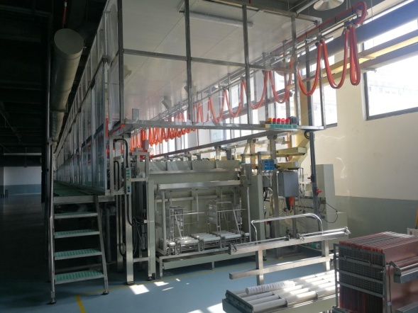
On a production line, electroless copper deposition is not one tank but a conveyor of ten or more, each doing one job. The table below summarizes a conventional horizontal sequence and what the line operator actually controls at each stage.
| Step | Purpose | Key Controls |
|---|---|---|
| 1. Deburr | Remove burrs around hole exits left by drilling | Brush pressure, feed speed |
| 2. Alkaline clean | Remove oils, fingerprints and drill dust; adjust surface charge positive | Bath concentration, temperature, dwell time |
| 3. Microetch | Strip oxides and roughen copper for adhesion | Persulfate or peroxide-sulfate chemistry, etch depth |
| 4. Predip | Protect the palladium bath; carry chloride into activation | Specific gravity, copper contamination limits |
| 5. Activation | Adsorb colloidal palladium onto walls and surfaces | Pd concentration, temperature, agitation |
| 6. Acceleration | Strip the tin shell to expose catalytic Pd nuclei | Acid type and strength, dwell time |
| 7. Electroless copper | Deposit the thin conductive seed layer | pH, temperature, Cu²⁺ and reducer concentration |
| 8. Rinse and dry | Stop the reaction, remove bath residues | Water quality, rinse cascade design |
| 9. Inspection | Confirm coverage before plating | Visual, continuity and coupon checks |
Two details in this sequence deserve attention when you audit a supplier. First, the clean-to-activation window: once a panel is cleaned and charged, it must reach the palladium bath before the surface re-contaminates, so conveyor speed and transfer timing are process parameters, not conveniences. Second, the microetch rate is measured in microns of copper removed per cycle — too little leaves oxide, too much attacks fine features. Both are documented in a well-run bath log.
Reading the Board: Hole Wall Before and After Deposition
The difference between an unprocessed and a processed panel is easy to see once you know what to look for. Before deposition, the hole wall blends into the laminate — a bare epoxy-glass surface with only the outer-layer copper foil visible at the panel faces. After deposition, every surface the chemistry touched carries a uniform, pinkish copper film, including the full length of each barrel.
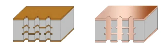
In cross-section, the seed layer is barely visible at production magnification — its real verdict arrives later, after electrolytic plating thickens the barrel. What inspection looks for at this stage is continuity: no bare patches, no thin streaks near the mid-plane of thick boards, and no glass fibers protruding where desmear was incomplete. A panel that passes here is safe to send to pattern plating; one that does not will carry the defect into every downstream step.
Common Electroless Copper Defects and Root Causes
Most plating-related field failures trace back to this step, and the failure modes are well understood. The table maps the four defects worth knowing as a buyer or engineer to the process parameter that usually causes them.
| Defect | Typical Root Cause | Prevention Focus |
|---|---|---|
| Hole-wall void | Activation miss or air trapped in the barrel during deposition | Wetting and agitation; clean-to-activate timing |
| Thin or patchy barrel | Bath out of range — pH, temperature or copper concentration drift | Scheduled titration and automatic dosing |
| Poor adhesion / peelers | Weak microetch or residual contaminant under the seed layer | Etch-rate control; cleaner bath maintenance |
| Hole-wall pull-away after thermal stress | Incomplete desmear leaving resin smear on the wall | Desmear verification before deposition |
Voids deserve special attention because they are invisible at final visual inspection — the barrel can look completely plated from outside while a thin gap remains mid-wall. That is why serious shops treat plating voids as a process-control problem rather than a sorting problem: monitor the bath, verify coverage on coupons, and only ship what the records support.
How Factories Verify PTH Quality
Verification happens at three levels. At the bath level, titration and solution analysis confirm that every chemistry stage sits inside its control window; a bath log with daily entries is one of the simplest things to ask a supplier for. At the panel level, continuity testing after plating confirms that every drilled hole conducts end to end.
At the metallurgical level, cross-sections and backlight inspection close the loop. A backlight test sends light through the plated barrel: a well-deposited wall glows uniformly, while voids or thin spots show up as dark breaks. Cross-sectioning production coupons measures final barrel copper thickness and plating uniformity against the order specification — this is the same evidence base referenced by IPC acceptance standards for plated-through-hole quality.
None of these checks can retroactively fix a bad deposition run, which is why the inspection burden is front-loaded in a capable plant. When you qualify a factory for a new multilayer product, asking how they sample coupons per panel and how often baths are analyzed tells you more than any marketing document.
Design Choices That Make Electroless Copper Easier or Harder
The deposition process is largely invisible to designers, but two design variables directly change its difficulty. The first is aspect ratio — board thickness divided by hole diameter. Deep, narrow barrels are harder to wet, harder to keep bubble-free, and harder to plate uniformly, which is why aspect ratio limits appear in every capability table. Specifying the largest drill your fanout allows is free reliability.
The second is hole type. Through-holes, blind vias and laser-drilled microvias each present different wetting and plating windows; HDI stacks with stacked microvias concentrate multiple deposition cycles into a few millimeters of board. Our HDI PCB technology guide covers how those builds sequence lamination and drilling, and why microvia metallization has its own dedicated process controls down to 0.1 mm laser holes.
Material choices matter at the margin too. High-glass-transition laminates and heavily filled resins change how the wall behaves in desmear, which shifts the optimal cleaner and microetch settings. None of this makes a design unbuildable — it just means the shop running your board should be adjusting the front end deliberately instead of running one recipe for everything.
Where Electroless Copper Sits in the Overall Build Flow
In a multilayer flow, deposition runs immediately after drilling and desmear, and before pattern plating and outer-layer imaging. Everything upstream — lamination quality, drilling condition, desmear — either sets up the step or sabotages it; everything downstream — final barrel thickness, hole reliability, assembly yield — inherits its result. It is the hinge point of the whole process.
That is also why it appears in so many of the failure analyses we publish. The same chemistry enables the outer-layer patterning and plating sequence on a conventional multilayer board and the fine-line builds described in our prototyping workflow. If you want to see the end results on real products, our 8-layer security system PCB and 4-layer SATA SSD PCB pages both show production boards whose layer-to-layer connections depend on this step.
For engineers reviewing a new stackup, the practical takeaway is simple: treat the front end as a system. Drill quality, desmear, deposition and plating are one continuous chain, and the factory that measures all four is the factory whose holes survive reflow and years in the field.
Frequently Asked Questions
What is electroless copper deposition in PCB manufacturing?
It is the chemical process that plates a thin copper seed layer onto the non-conductive hole walls of a drilled PCB without applied current. Palladium catalyst activated by the line makes the insulating surface plateable, and the resulting film serves as the base for electrolytic copper that builds the final plated-through-hole barrel.
Why is palladium used in the PTH process?
Colloidal palladium is one of the few practical catalysts for electroless copper. The particles adsorb onto a properly cleaned and charged hole wall, then an acceleration bath strips their stabilizing tin shell to expose active palladium nuclei. On those nuclei, copper ions are reduced chemically by formaldehyde, so deposition starts exactly where the catalyst landed.
How thick is the electroless copper layer?
The chemical deposit is a seed layer, typically a few tenths of a micron — far below final barrel thickness. Its job is conductivity and continuity, not current carrying. Electrolytic plating immediately afterward brings the barrel to its specified final thickness, commonly in the range of 20 to 30 microns depending on the order requirement.
What is the difference between electroless copper and electrolytic copper plating?
Electroless copper needs no external current: deposition is driven by a chemical reducing agent on catalyzed surfaces, which is why it can plate inside an insulating hole wall. Electrolytic plating uses applied current and can only deposit on conductive surfaces. Production through-holes need both — the chemical seed first, then electroplating to build thickness and fill.
What causes voids in plated through holes?
Most barrel voids trace to a missed or weakened step before plating: incomplete activation, air trapped in the barrel, drill smearing that blocked catalyst adsorption, or a bath drifting out of its control window. Because the defect forms at the seed stage, prevention means bath monitoring, wetting control and coupon verification rather than final inspection.
Does electroless copper deposition apply to HDI microvias?
Yes. Laser-drilled microvias — down to 0.1 mm in modern HDI builds — are metallized by the same chemical deposition chemistry, usually with dedicated line parameters for wetting and plating uniformity in small geometries. Stacked and staggered microvia structures simply repeat the drill-desmear-deposit cycle at each stage of the HDI stackup.
How does aspect ratio affect through-hole plating quality?
Aspect ratio is board thickness divided by drill diameter. High values mean deep, narrow barrels that are harder to wet, harder to keep free of trapped air and harder to plate uniformly along the full length. Keeping aspect ratio within the manufacturer’s stated window — or upsizing drills where routing allows — is the cheapest reliability improvement a designer can make.
Get Your Stackup and Hole Specs Reviewed Before Prototyping
If your board combines high aspect-ratio holes, back-drilling candidates or an HDI stack, send the Gerber data and stackup draft for an engineering review before you commit to fabrication. Our team will confirm aspect ratios, annular rings and plating requirements against current line capability, and flag anything that would put the manufacturing process under avoidable stress. Submit your files through the quote request page and you will receive a manufacturability response with a firm lead time confirmed at engineering review.