Book Appointment Now

The PCB prototyping process stage by stage, the DFM checks that prevent rebuilds, and what to verify before a prototype run commits to volume.
PCB Prototyping Process: From Gerber Files to First Article
A prototype is the cheapest place to find a mistake. The PCB prototyping process turns your Gerber files into first articles that prove a design before tooling decisions and volume schedules are committed — and the difference between a smooth run and a rebuild is mostly decided before the first panel is ever cut. This guide follows a prototype order stage by stage, from file review through electrical test and shipment, and tells you what to verify at each handoff.
It is written for hardware engineers and the people who buy for them: what actually happens inside the fab, which checks prevent the expensive failures, and how to judge a prototyping partner on more than the number at the bottom of the quote.
Table of Contents
- What a Prototype Buys You Before Volume Commitment
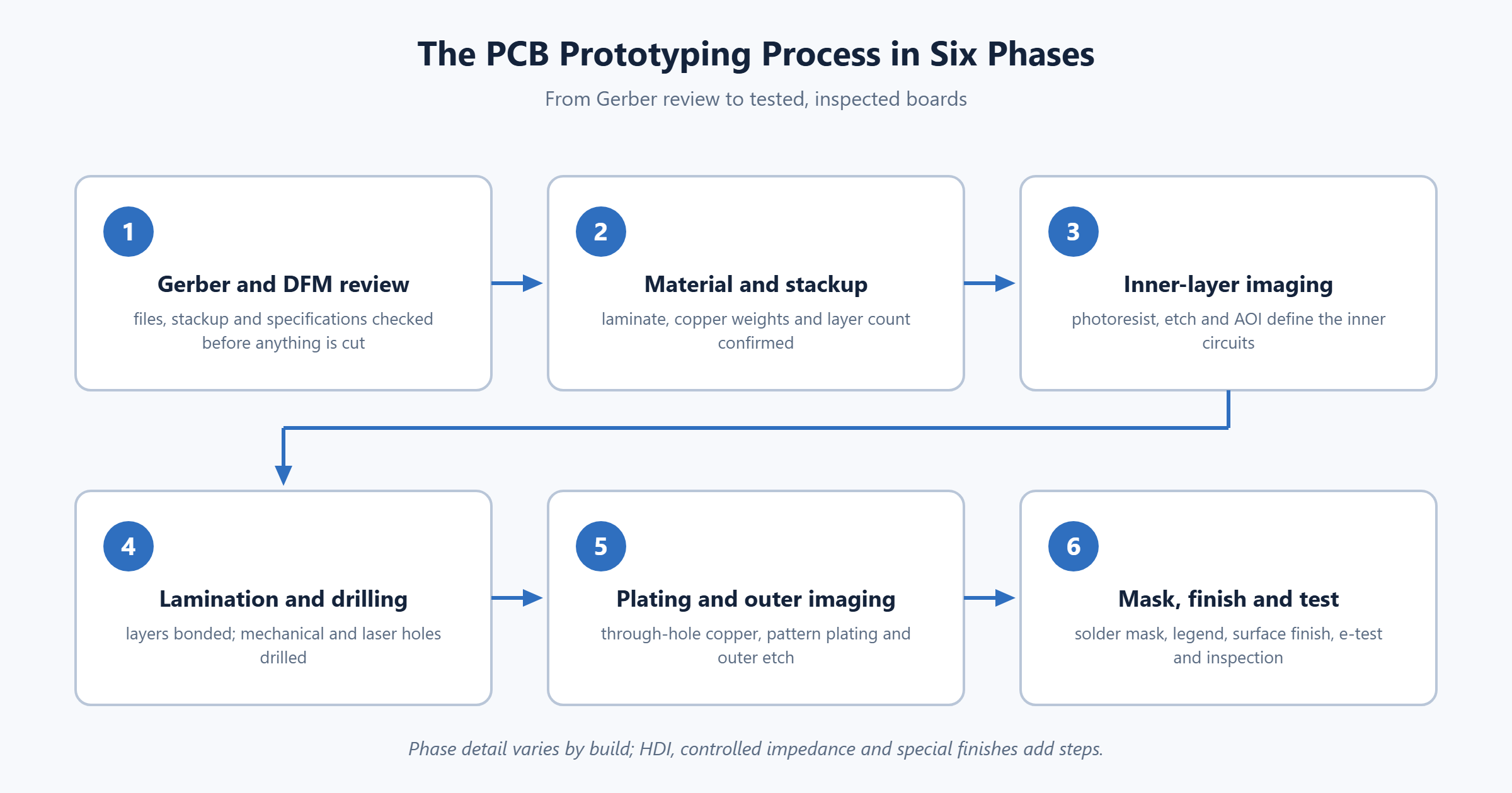
- The PCB Prototyping Process, Stage by Stage
- Front-End DFM Review: The Checks That Prevent a Rebuild
- Material and Stackup Choices for a Prototype Run
- Holes, Plating and Layer-to-Layer Registration
- Solder Mask, Legend and Surface Finish Selection
- Electrical Test, Final Inspection and the Report
- How to Evaluate a PCB Prototyping Partner
- Cost Drivers and Turnaround in Prototype Quantities
- Where the PCB Prototyping Process Usually Goes Wrong
- FAQ
- Submit Your Gerber Files for an Engineering Review
What a Prototype Buys You Before Volume Commitment
A prototype run answers questions that simulation cannot close on its own: does the board fit the enclosure, can the fabricator hold your impedance targets on this stackup, do the footprints match the parts actually purchased, and does the assembly behave thermally the way the model predicted. Each of those questions is dramatically cheaper to answer on ten boards than on ten thousand.
There is a second, less obvious return. A prototype forces the design data into final form — complete stackup, defined finishes, marked controlled impedances — which is exactly the data set a volume fab will demand later. Teams that prototype rigorously move into mass production without a documentation scramble, because the handoff package was already tested once.
Design data itself still moves between tools and fabs as Gerber data, the format maintained by Ucamco. File integrity is therefore the first quality gate of the whole process: a fabrication package that opens cleanly, matches the drill files, and carries an explicit stackup is already ahead of most orders that get rescheduled.
The PCB Prototyping Process, Stage by Stage
Inside the fab, a prototype order moves through the same production line as a volume order — just in smaller panels with more engineering attention. The table below lists the classic production sequence and, more usefully, what you as the customer should verify at each stage.
| Stage | What happens | What to verify |
|---|---|---|
| 1. Front-end review | DFM check, stackup and specification review, production MI created | MI matches your fab drawing, not a default |
| 2. Material cutting | Laminate sheared into production panels | Material brand and grade as specified |
| 3. Drilling | Mechanical and laser holes drilled per program | Hole sizes and layer registration |
| 4. Electroless copper | Thin copper deposited on hole walls | Continuous coverage before plating |
| 5. Pattern transfer | Circuit image transferred onto the panel | Artwork derived from your Gerber, unaltered |
| 6. Pattern plating | Copper built up on circuits and in holes | Plating thickness meets class requirement |
| 7. Stripping and etching | Resist removed, excess copper etched away | Resulting line width and spacing |
| 8. Solder mask | Mask imaged, developed and cured | Alignment on fine-pitch pads |
| 9. Legend | Reference designators and marks printed | Polarity and first-pin marks legible |
| 10. Surface finish | ENIG, HASL, OSP or other finish applied | Finish matches the assembly process |
| 11. Profiling | Board routed or scored to final outline | Outline dimensions and edge quality |
| 12. Electrical test | 100% open and short testing | Test report with actual coverage |
| 13. Final inspection | 100% visual inspection against the class criteria | Acceptance class agreed up front |
| 14. Packing and shipment | Vacuum packing with documentation | Certificates included in the box |
Special technologies extend this backbone rather than replace it. HDI adds laser drilling and stacked via steps after stage 3; rigid-flex adds lamination and book-binding complexity; heavy copper changes the plating windows. The sequence logic stays the same, which is why a supplier who runs the standard sequence well usually runs the extensions well too.
Front-End DFM Review: The Checks That Prevent a Rebuild
Everything before stage 2 is paper, and it is where the majority of schedule disasters are actually prevented. A serious design-for-manufacturing review checks the package as a system, not as isolated files.
- File completeness: Gerber layers, drill files, and a stackup table that all agree on layer count and copper weights.
- Annular rings: pad sizes against finished hole sizes, with the class requirement made explicit.
- Line and space: requested trace geometry compared against published capability, with controlled-impedance nets flagged.
- Hole-to-copper clearance: non-plated and plated hole clearances checked against layer nesting.
- Impedance targets: a stackup proposal with calculated values before material is ordered.
- Special processes: filled vias, blind and buried structures, heavy copper — flagged so the line plans for them.
The output of a good review is questions, not just a confirmation. If a fabricator returns a DFM report with specific findings — a net with 5 mil spacing against an 8 mil request, an annular ring that only closes on one layer — that is a supplier worth keeping. Our own PCB manufacturing capability page exists for exactly this reason: check the numbers before the order, not after the first scrap report.
Material and Stackup Choices for a Prototype Run
Material selection is where prototypes most often drift from what the design intended. Standard FR-4 is the correct default for the majority of digital boards, but the exceptions are predictable, and they are worth naming before the order is placed rather than after the first reflow.
| Design requirement | Material direction | Notes |
|---|---|---|
| Standard digital logic | Mid-loss FR-4 | The cost-effective default for most builds |
| Elevated operating temperature | Laminate with Tg 150–180 | Match glass transition to reflow and service temperature |
| High-speed or RF signals | Low-loss laminate | Controlled Dk and dissipation factor for predictable impedance |
| High insulation demand, harsh environment | High-CTI laminate | Higher comparative tracking index supports smaller creepage margins |
| Mixed digital and RF | Hybrid stackup | Balances performance and cost per layer; see hybrid build guidance |
Two references make this decision easier. The PCB materials and laminates guide explains how resin systems, glass styles and copper foil roughness change behavior, and the PCB material selection guide walks the choice from standard FR-4 through low-loss options. For a prototype, the practical rule is simple: prototype on the material you intend to build with in volume, because impedance and thermal behavior do not translate between resin systems.
Holes, Plating and Layer-to-Layer Registration
Holes are where a multilayer earns or loses its reliability. Mechanical drilling defines the plated through-holes; laser drilling defines the microvias on HDI builds. Both feed into electroless copper for the seed layer, then electroplating to bring the barrel to its final thickness. The plating thickness in the barrel is not a detail — it is the conductor that connects your layers, and it follows the same class criteria as the surface copper.
Registration is the quiet variable. Every layer is imaged and etched separately, then stacked and laminated; the tolerance of that stacking decides how much margin your annular rings actually have. A design with generous hole-to-copper clearance tolerates normal registration drift invisibly, while a design that spends every last mil will show it as breakout on the cross-section. When a prototype cross-section report is offered, the registration and barrel quality in it are the two items to read first.
Aspect ratio ties the whole hole story together. Deep, narrow holes plate unevenly because current struggles to reach the barrel center, so capable fabs hold aspect ratios within published windows. On our floor, blind microvias run at 0.1 mm with a 1:1 aspect ratio as standard, and buried via structures are planned around the same logic.
Solder Mask, Legend and Surface Finish Selection
Solder mask looks like a cosmetic choice and behaves like an electrical one. Mask definition on fine-pitch pads decides whether assembly gets clean, flat solderable surfaces or masked-over toes; dam sizes between balls on a dense BGA matter more than the mask color. For prototypes destined for assembly, specify mask alignment expectations rather than accepting defaults.
Surface finish is the other decision that reaches into assembly. ENIG gives flat, solderable pads and long shelf life, which suits fine-pitch and BGA work. HASL remains economical for through-hole-heavy boards but leaves an uneven surface. OSP is cost-effective where paste coverage is controlled and shelf life is short. When a build needs wire bonding or repeated assembly cycles, upgraded finishes enter the conversation — the trade-offs are laid out in this ENEPIG surface finish comparison.
The legend finishes the board for humans. Reference designators, polarity marks, first-pin indicators and date codes cost almost nothing at order time and save real assembly errors later. The one rule: put legend requirements in the fab drawing, because a legend added from memory at the end of the process is where omissions happen.
Electrical Test, Final Inspection and the Report
Electrical testing is the last process step that can catch a functional defect before you can. Every board should be tested 100% for opens and shorts against the netlist derived from your data. Volume orders typically use dedicated test fixtures; prototype quantities more often run on flying-probe systems, which trade cycle time for the absence of fixture cost — the right economics at small quantities, and worth confirming rather than assuming.
Final inspection is 100% visual against the acceptance class the order specifies. Class 2 electronics and Class 3 high-reliability differ concretely in allowed plating nodules, mask defects and conductor imperfections, and the difference is defined in the IPC-6012 performance specification family. Agreeing the class at order entry is what makes inspection meaningful — an inspection without a stated class is an opinion, not a test.
The documentation package is part of the product. A test report, the dimensional or cross-section data where specified, and a certificate of conformance let your team close the loop without re-measuring everything in-house. Our IPC-A-600 Class 3 requirements walkthrough shows which visual criteria matter most if you are specifying high-reliability acceptance for the first time.
How to Evaluate a PCB Prototyping Partner
Prototype suppliers are easy to compare on price and nearly impossible to compare on risk from the outside. The criteria below convert the invisible parts of the service into checkable questions.

| Criterion | Why it matters | What good looks like |
|---|---|---|
| Engineering feedback | Catches DFM issues before they become scrap | A DFM report with specific findings and questions, not just a price |
| Capability match | Avoids switching suppliers mid-project | Published capability data including HDI stages and impedance control |
| Test coverage | Opens and shorts otherwise surface in your lab | 100% electrical test with a report per order |
| Process traceability | Links each panel to its process data | Batch records and certificates with every shipment |
| Communication | Schedule surprises need early escalation | A named contact who answers before you chase |
Scale and stability sit behind all five rows. Season Multilayer Circuit (Shenzhen) Co., Ltd. is part of 998 PCB Group, founded in 2006, with 3,000,000 m² of annual capacity across plants in Shenzhen, Jiangxi and Anhui, building boards from 2 to 30 layers. The relevance to a prototype buyer is direct: the line that builds your ten boards is the same infrastructure that builds your volume, so capability proven at prototype scale carries over. The engagement model is described on our PCB manufacturing services page.
Cost Drivers and Turnaround in Prototype Quantities
In the PCB prototyping process, pricing behaves differently from volume because setup dominates. Tooling, programming, drilling setup and test setup are paid whether the order is ten boards or a hundred, so small quantities carry a high per-board share of fixed cost. Understanding that structure explains most cross-quote differences: a quote that looks cheap may simply be excluding a setup step you will pay for later.
The variable cost drivers are the familiar ones: layer count, material grade, hole count and the smallest hole sizes, surface finish, and controlled impedance, which adds stackup engineering and test coupons. Each moves cost on a multiplier basis rather than linearly, which is why one material upgrade can reshape a quote. The breakdown logic is the same one detailed in this PCB cost drivers and quote checklist.
Turnaround follows the process chain, not ambition. A simple 2-layer board moves through the sequence in a handful of working days; an 8–10 layer 2-Stage HDI prototype typically runs on the order of 17–18 working days, with the confirmed schedule issued at engineering review. Ask what is included in the quoted turnaround — inspection depth and electrical test are the two items most often compressed when a schedule is tight.
Where the PCB Prototyping Process Usually Goes Wrong
Most prototype rebuilds trace back to the handoffs, not the fabrication itself. The recurring offenders are short enough to list.
- Incomplete file packages — missing drill files or a stackup that contradicts the Gerber layers.
- Unstated impedance targets — discovered after fabrication when the stackup cannot be changed.
- Footprint drift — the board was designed against one package revision while purchasing ordered another.
- Finish mismatch — a finish chosen for price that the assembly process or shelf life cannot live with.
- Legend omissions — polarity and first-pin marks left out, then improvised in assembly.
- Skipped test reporting — electrical test passed silently, with no report to compare against field data.
Each of these is preventable with the checks in the DFM and handoff sections above, which is why the front end of the process deserves more attention than it usually gets. When a defect does escape, the acceptance criteria you agreed at order entry decide how the claim is resolved — one more reason to put the class and the report requirements in writing before the build starts.
Frequently Asked Questions
What are the main stages of the PCB prototyping process?
The backbone sequence runs: front-end DFM review, material cutting, drilling, electroless copper, pattern transfer, pattern plating, etching, solder mask, legend, surface finish, profiling, 100% electrical test, final inspection and packing. HDI builds add laser drilling and stacked via steps, and special finishes or heavy copper extend the plating stages. The sequence is identical to volume production, scaled to smaller panels.
Which files do I need to submit for a PCB prototype order?
At minimum: complete Gerber layers, drill files, and a stackup table with copper weights and dielectric properties. A fabrication drawing with the acceptance class, surface finish, and legend requirements removes ambiguity, and a netlist enables true electrical test. Impedance-controlled designs should also state target values per layer pair so the stackup can be engineered before material is ordered.
How long does a PCB prototype take?
It depends on complexity. A simple 2-layer board typically moves through the full process in a handful of working days. An 8–10 layer 2-Stage HDI prototype with filled, stacked microvias typically runs on the order of 17–18 working days. Every schedule is confirmed at engineering review for the specific design, so treat quoted turnarounds as process-driven rather than fixed.
How many prototype boards should I order?
Order what the validation plan actually needs: boards for bring-up, boards for assembly trials, spares for rework and a few held in reserve for the fixes the first build will reveal. Because setup costs dominate small quantities, the per-board price difference between a slightly larger and a minimal quantity is often small compared with the cost of ordering again two weeks later.
What is a DFM review and why does it matter before prototyping?
A design-for-manufacturing review checks your files against the fabricator’s real capability: annular rings, line and space, hole-to-copper clearance, aspect ratios and stackup feasibility. It matters because the review is where rebuilds are prevented — a spacing violation caught in review costs a file edit, while the same violation caught on finished boards costs a full re-run and a slipped schedule.
How is a prototype different from a production order?
The fabrication sequence of the PCB prototyping process is the same as volume production; what changes is scale and emphasis. Prototypes run in smaller panels, often on flying-probe electrical test instead of a dedicated fixture, with more engineering attention per panel. Production adds panel utilization optimization and formalized process capability data. A good prototype therefore doubles as a process validation, not just a design check.
How do I choose a PCB prototyping supplier?
Judge on the checks that predict risk: a DFM review that returns specific findings, published capability data that matches your technology, 100% electrical test with reports, traceable process documentation, and a named engineering contact. Then consider scale — a supplier whose prototype line sits inside the same infrastructure as volume production, backed by real capacity, carries your design forward without a second qualification effort.
Submit Your Gerber Files for an Engineering Review
Send your Gerber data, drill files and stackup, and you will get back an engineering review with concrete findings — capability checks against your design rules, a stackup proposal for any controlled impedances, and a confirmed schedule for the actual build. The review happens before anything is cut, which is the cheapest possible place to fix a problem. Start on our PCB manufacturing services page and include your target quantities; they change the test and tooling recommendations more than any other single input.