Book Appointment Now

High-frequency PCB explained: what Dk and Df really control, material families compared, hybrid FR-4 stackups, manufacturing impacts and a 5-step material screen.
High-Frequency PCB: Materials, Dk/Df and When to Spec Them
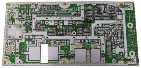
A high-frequency PCB is not defined by how many layers it has or how fine its traces are — it is defined by how the board behaves when signal wavelengths shrink to the size of the traces themselves. Above roughly a few hundred megahertz, an ordinary laminate stops being invisible: dielectric loss, impedance drift and copper roughness start eating margin that no redesign downstream can win back. The result is usually the same story — a board that passes continuity tests but fails in the field.
This guide explains what actually separates a high-frequency PCB from a standard digital board: the two material numbers that decide performance, how the main laminate families compare, when a hybrid FR-4 stackup is the smarter buy, how RF work changes manufacturing decisions, and a practical five-step screen for choosing material on your next build. If you want the full material landscape first, start with our PCB materials and laminates guide, then come back here for the RF-specific decisions.
Table of Contents
- What Is a High-Frequency PCB?
- Where High-Frequency PCBs Are Used
- Dk and Df: The Two Numbers That Decide Performance
- High-Frequency PCB Material Families Compared
- Hybrid Stackups: FR-4 With RF Layers
- How a High-Frequency PCB Changes Manufacturing
- Impedance Control and Test Coupons for RF Builds
- Choosing a High-Frequency PCB Material: A 5-Step Screen
- What Drives High-Frequency PCB Cost
- FAQ
- Send Your RF Stackup for an Engineering Review
What Is a High-Frequency PCB?
A high-frequency PCB is a board engineered to carry radio-frequency signals — typically from hundreds of megahertz into the tens of gigahertz — with predictable impedance and minimal loss. The definition is about electrical behavior, not a layer count: an antenna feed on two layers can be far more demanding than a twelve-layer digital board. What changes at RF is that the laminate itself becomes a circuit element, and every material property that digital designers can ignore becomes a specification.
Three properties dominate. Dielectric constant (Dk) sets the velocity and the geometry of every transmission line. Dissipation factor (Df) sets how much of the signal turns into heat on the way down the trace. And the consistency of both across the panel, across frequency and across temperature decides whether your filter or antenna still performs at the edges of its band. A high-frequency PCB is, in practice, a material choice first and a routing exercise second.
Where High-Frequency PCBs Are Used
The application list reads like a map of the radio spectrum. In communications infrastructure, base station power amplifiers and antenna arrays run high power at microwave frequencies, where laminate loss converts directly into heat and coverage. Automotive radar puts 77 GHz front ends behind a bumper, where temperature stability of Dk matters as much as its absolute value. Satellite and GNSS receivers, backhaul links, industrial RF sensing, medical imaging radios and lab test equipment all live in the same regime — signal integrity is the product, and a high-frequency PCB is the product, not a component.
Two commercial consequences follow from that list. First, RF boards are usually low-volume, high-mix products, so the fabricator you choose matters more than the unit price: a supplier who runs radar high-frequency PCB builds week in and week out has already paid for the learning curve your project would otherwise fund. Second, RF and digital circuitry increasingly share one board, which pushes designs toward the hybrid constructions described later in this guide.
Dk and Df: The Two Numbers That Decide Performance
Dielectric constant determines how fast a signal travels and, together with trace geometry, what impedance a line has. A tighter Dk tolerance means your 50-ohm line is 50 ohms on every panel, not just on average. Dissipation factor determines dielectric loss — at 1 GHz an ordinary FR-4 loses a manageable fraction of signal energy, but the loss climbs roughly with frequency, which is why a design that simulates fine at 900 MHz falls apart at 6 GHz on the same material. On a high-frequency PCB, that loss curve is the first thing to check.
The table below gives the practical ranges engineers quote when screening materials. Treat them as screening bands rather than datasheet values — each laminate grade has its own exact figures, and Dk varies with resin content, glass style and frequency.
| Parameter | Standard FR-4 | Hydrocarbon-ceramic (e.g. Rogers RO4000 series) | PTFE-based |
|---|---|---|---|
| Dk (design value) | ≈ 4.2–4.6 | ≈ 3.0–3.5 | ≈ 2.1–3.0 |
| Df (typical) | ≈ 0.015–0.025 | ≈ 0.002–0.004 | ≈ 0.001–0.003 |
| Dk stability vs temperature | Moderate | Good | Excellent |
| Loss at 10 GHz | High | Low | Very low |
| Processing similarity to FR-4 | — | Close (standard PTH line | Different (special drilling/desmear) |
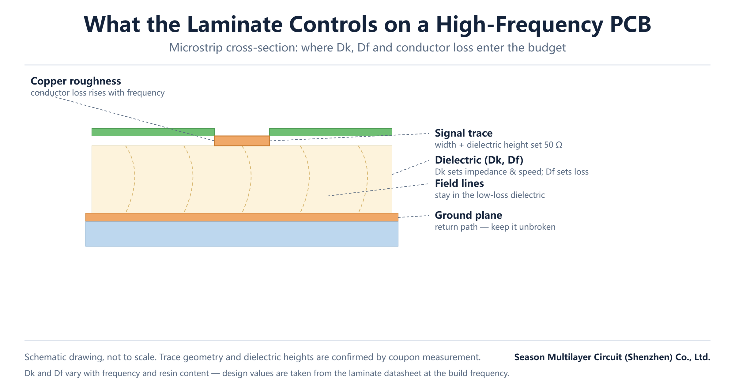
One caution: Dk values quoted at 1 MHz do not describe behavior at 10 GHz. Serious laminates publish Dk by frequency and by resin content, and a fabricator running controlled-impedance work should model your lines with the frequency-appropriate value — then verify on a coupon. Callouts and test conventions for RF laminates follow the IPC base material specifications.
High-Frequency PCB Material Families Compared
RF laminates fall into a few engineering families, and knowing which family a datasheet belongs to tells you most of what you need about cost and manufacturability. Hydrocarbon-ceramic materials — the family behind the well-known Rogers RO4350B and RO4003C grades — were designed specifically to process like FR-4 while performing like microwave laminates, which is why they dominate commercial RF work. PTFE-based materials push electrical performance further and cost and handling difficulty with it.
| Family | Electrical performance | Manufacturability | Relative cost | Typical use |
|---|---|---|---|---|
| Standard FR-4 | Usable to roughly 1–2 GHz | Baseline | Reference | Cost-sensitive radios, low-GHz IoT |
| Hydrocarbon-ceramic | Low loss into the tens of GHz | Processes on a standard line | Moderately above FR-4 | Base station, automotive radar, backhaul |
| PTFE with ceramic filler | Very low loss, stable Dk | Special drilling and desmear | Well above FR-4 | mmWave radar, satellite, test equipment |
| Pure PTFE | Best available loss and Dk control | Most demanding process window | Highest | .mmWave front ends, metrology |
We run all of these families in production — Rogers-class hydrocarbon ceramics, PTFE-based and filled-PTFE grades — so the family choice is an engineering decision, not a capability constraint — and most commercial grades in both families carry UL recognition for flammability and long-term reliability. A worked example of the double-sided end is our Rogers high-frequency PCB product build, and the screening logic that gets you from an application to a family is the five-step method at the end of this article.
Hybrid Stackups: FR-4 With RF Layers
Full-stack PTFE is rarely necessary. The workhorse construction for mixed RF-plus-digital products bonds one or two microwave-grade layers — where the antennas, filters and transmission lines live — onto standard FR-4 cores that carry power, control and logic. The RF signals see the low-loss dielectric; everything else rides on inexpensive, well-understood laminate. Cost lands between the two extremes, often dramatically closer to FR-4 than to a full PTFE build.
The engineering price of a hybrid is at the interfaces: dissimilar materials expand and cure differently, so lamination schedules, desmear chemistry and reliability validation all need to account for the pairing. Done by a fabricator who has run the combination before, a hybrid stackup is routine; done by one meeting the material pairing for the first time, it is a qualification project — and the reliability of a hybrid high-frequency PCB lives or dies at those interfaces. See our hybrid stackup guide for the design rules, and our PCB laminate selection guide for how RF choices fit the wider material decision.
How a High-Frequency PCB Changes Manufacturing
Manufacturing a high-frequency PCB tightens tolerances across the whole line, not just at etch. Impedance-sensitive traces need tighter etch control than power or digital routing. Dielectric thickness on RF layers is controlled to a fraction of what a digital layer pair needs, which drives prepreg selection and press scheduling. And material choice ripples into drilling and hole preparation: PTFE laminates need plasma desmear and different drill parameters from epoxy systems.
| Process area | Standard FR-4 practice | High-frequency practice |
|---|---|---|
| Etch compensation | Standard line-width budget | Tighter control on RF traces; coupon-verified |
| Prepreg selection | Generic build-up per thickness | Chosen per layer pair for dielectric and fill |
| Drilling / desmear | Standard epoxy parameters | PTFE grades need plasma desmear and revised feeds |
| Surface finish | Chosen by assembly needs | Also screened for RF loss — thin finishes preferred |
| Inspection | AOI plus electrical test | Adds impedance coupons, and X-ray on RF regions |
Surface finish deserves a specific note: thick nickel under ENIG adds loss at high frequencies, which is why some RF designs prefer thin immersion silver or OSP on RF layers while keeping ENIG where wire bonding or pad wear demands it. There is no universal answer — the finish is chosen with the frequency band and assembly process in view, and the decision belongs in the stackup review, not after routing.
Impedance Control and Test Coupons for RF Builds
On a high-frequency PCB, controlled impedance stops being a formality. Single-ended 50-ohm lines and 100-ohm differential pairs are simulated from the actual stackup, then verified on a coupon that carries the same construction — same dielectric heights, same copper weights, same trace geometry — processed alongside the production panel. The coupon is measured with TDR or a VNA, and the numbers are compared against the agreed tolerance before the batch ships.
For RF work the tolerance conversation matters as much as the measurement. Standard digital builds commonly run ±10%; RF transmission lines are frequently held to ±8% or tighter where the design needs it, and the honest answer about what is achievable comes from engineering review, not from a quote checkbox. Our impedance measurement methods guide covers the instruments and the coupon design behind those numbers.
Choosing a High-Frequency PCB Material: A 5-Step Screen
Material selection for a high-frequency PCB goes wrong when it starts from the datasheet instead of the requirements. The screen below runs in the opposite direction and takes minutes, not weeks — and it prevents the two classic mistakes: buying microwave performance a design does not need, and discovering loss budget problems after the layout is frozen.
- Fix the frequency band and loss budget. A 900 MHz sensor and a 28 GHz front end have nothing in common; write the highest frequency of consequence and the tolerable insertion loss down first.
- Set the thermal environment. Automotive engine bays and outdoor base stations shift Dk; pick a family with the temperature stability the band needs.
- Decide mixed-signal scope. If digital lives on the same board, price a hybrid stackup against a full RF build before committing.
- Check assembly and rework demands. High-Tg assembly profiles, lead-free reflow and rework expectations constrain material choice as much as electricals do.
- Confirm fabrication experience. Ask which of the candidate grades your fabricator runs today, and ask for a coupon-based impedance report from a comparable build.
Run honestly, the screen usually lands on a hydrocarbon-ceramic grade for commercial RF and a PTFE construction only where the band or the loss budget forces it. Both are production-regular processes for us, and our materials guide covers how these families sit alongside the rest of the laminate range.
What Drives High-Frequency PCB Cost
High-frequency PCB cost is dominated by three levers, in order: material, yield and test. The laminate itself typically carries a multiple of FR-4 pricing — modestly for hydrocarbon ceramics, substantially for filled PTFE grades — and it scales with panel area consumed. Yield is the second lever: RF builds with tight etch and impedance tolerances scrap more panels, and that margin is priced in. Test is third: coupon fabrication and TDR or VNA verification add real steps to the flow.
The controllable insight is that over-specification is the most common cost amplifier. Moving from FR-4 to a low-loss ceramic grade because a design simulates poorly, when the real problem is an unmolded reference plane or a lossy connector transition, multiplies material cost without fixing the fault. Conversely, forcing a millimeter-wave design onto ordinary laminate to save material budget reliably produces boards that pass electrical test and fail in deployment. Getting the engineering review before the quote is what separates the two outcomes — and it costs nothing but a stackup.
Frequently Asked Questions
What frequency counts as a high-frequency PCB?
There is no single cutoff, but designs above roughly a few hundred megahertz start depending on laminate properties, and above 1–2 GHz standard FR-4 loss becomes a design constraint. Most engineers treat anything into the GHz range as RF territory where a high-frequency PCB material choice is on the table.
Is Rogers material always required for RF boards?
No. Below roughly 1–2 GHz, carefully stacked FR-4 often meets the loss budget. Between those bands and tens of GHz, hydrocarbon-ceramic grades such as the Rogers RO4000 series are the commercial default, and PTFE constructions take over for the most demanding millimeter-wave work. The band and loss budget decide, not the brand name.
What is the difference between Dk and Df?
Dk (dielectric constant) sets signal velocity and the trace geometry needed for a target impedance. Df (dissipation factor) sets how much signal energy the dielectric converts to heat — the loss that grows with frequency. In practice Dk determines impedance accuracy and Df determines how far a signal survives; both must be stable across frequency and temperature for RF use.
Can a high-frequency PCB use FR-4 inner layers?
Yes — that is exactly what a hybrid stackup does. One or two microwave-grade outer or buried RF layers are bonded to FR-4 cores carrying the digital and power circuitry. It keeps RF performance where it matters while containing cost, provided the fabricator has qualified the material pairing for lamination, desmear and reliability.
Which surface finish is best for RF boards?
Thick nickel under ENIG measurably adds loss at high frequencies, so RF-heavy designs often specify thin finishes such as immersion silver or OSP on RF layers. Where wire bonding or pad durability is required, ENIG remains common with the nickel thickness taken into account in the loss budget. The choice belongs in the stackup review with the frequency band in view.
How is a high-frequency PCB verified before shipment?
Through impedance coupons built with the production stackup and measured with TDR or a VNA, plus AOI and electrical test. RF builds may add cross-sections on RF layer pairs and verification of dielectric thickness. The coupon report — measured values against agreed tolerance — is the document to request with every RF batch.
What should an RF PCB quote request include?
The material grade with its class (hydrocarbon-ceramic or PTFE-based), the full stackup with dielectric thicknesses, the impedance spec table with target and tolerance, copper weights on RF layers, surface finish per layer set, and the highest frequency of consequence. With those five items a fabricator can quote engineering reality instead of guessing.
Send Your RF Stackup for an Engineering Review
Material choice, hybrid construction and impedance tolerance interact — and they are cheapest to settle before routing freezes. Our engineering team reviews RF stackups against the band, loss budget and assembly process, then quotes what the build actually needs.
Submit your Gerber and RF requirements through our PCB manufacturing services page — high-frequency laminates from hydrocarbon-ceramic to PTFE families, with impedance control confirmed per engineering review.