Book Appointment Now

A practical checklist for choosing a multilayer PCB manufacturer: difficulty tiers, process questions, lead-time checks, certifications and RFQ tips.
How to Choose a Multilayer PCB Manufacturer: 5-Step Checklist
Searching for a multilayer PCB manufacturer returns a long list of names, and every one of them claims 2–30 layers, fast prototypes and full certification. The list proves nothing. The differences that actually matter — real layer capability, impedance precision, lead times that hold, and inspection that catches problems before shipment — only surface when you ask evidence-based questions, and they surface too late if you wait until after the production order. Most sourcing failures in multilayer work trace back to a selection step that relied on a list instead of a checklist.
This article turns supplier selection into five verifiable steps: place your board in a difficulty tier, put four process questions to each candidate, check prototype-to-production lead times, collect certification and inspection documents, and send one complete RFQ package. Every step ends with something you can put in front of a supplier and ask them to prove. If you are evaluating quotes right now, the checklist below is written to be used as-is.
Table of Contents
- Rank Your Board by Difficulty Tier Before You Shortlist Anyone
- What to Verify Before Shortlisting a Multilayer PCB Manufacturer
- Prototype-to-Production Lead Times: Get the Numbers in Writing
- Certifications and Outgoing Inspection: Two Documents to Collect
- The RFQ Package: Send It Complete, Once
- Validate with a Small Trial Order Before Production
- Red Flags When Screening a Multilayer PCB Manufacturer
- Matching Board Tier to Supplier Evidence
- FAQ
- Get Your Stackup Reviewed Before You Commit
Rank Your Board by Difficulty Tier Before You Shortlist Anyone
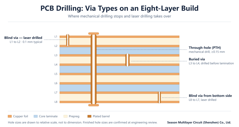
The first move is not collecting names. It is placing your build into a difficulty tier, because the tier decides which suppliers can realistically bid. A conventional 4–8 layer through-hole board is within reach of most established fabricators. Ten to sixteen layers with controlled impedance, or heavier copper than standard, narrows the field. Twenty-plus layers, blind and buried vias, or HDI builds narrow it further — and getting this ranking wrong is why a supplier that ships excellent 4-layer work can still fail an 18-layer build.
| Difficulty tier | Typical build | What to verify first |
|---|---|---|
| Entry tier | 4–8 layer through-hole boards on conventional FR-4 | Production layer count, standard prototype lead time, and batch-to-batch consistency on a small trial order |
| Advanced tier | 10–16 layers, controlled impedance, higher-Tg laminates | Impedance tolerance commitments and stackup proposal quality — a competent supplier returns a stackup recommendation with the quote |
| High-difficulty tier | 20+ layers, heavy copper, blind/buried vias or HDI | Maximum layer count, laser via capability and comparable shipped references; prototype before any production commitment |
Layer capability is the first number to pin down. A meaningful benchmark for a general-purpose fabricator is multilayer production in the 2–30 layer range, with prototype builds beyond 30 layers handled case by case at engineering review — that is the range we publish ourselves, and it is the range where most commercial and industrial products live. Ask each candidate for a comparable shipped reference at your layer count, not just the number on the website. Our 8-layer security system PCB is an example of the entry-to-advanced boundary in series production; if a supplier cannot show anything comparable, treat the gap as a finding, not a detail.
What to Verify Before Shortlisting a Multilayer PCB Manufacturer
Every supplier says they can build multilayer boards. The precision behind that sentence varies enormously, and the variation hides inside four process parameters. The table below turns each one into a question that separates documented capability from marketing copy — a structured multilayer PCB manufacturer evaluation can be finished in a ten-minute call per supplier.
| Check | Typical capability benchmark | The question that gets a real answer |
|---|---|---|
| Layers and board thickness | Production 2–30 layers; prototype builds to 64 layers per engineering review; finished thickness 0.2–6.0 mm | Do you have a shipped production board at my layer count and thickness? |
| Line width and spacing | 3/3 mil on conventional multilayer; 2/2 mil on HDI builds (1.8/1.8 mil achievable on prototypes) | Which trace-and-space class does my design fall into, and at what expected yield? |
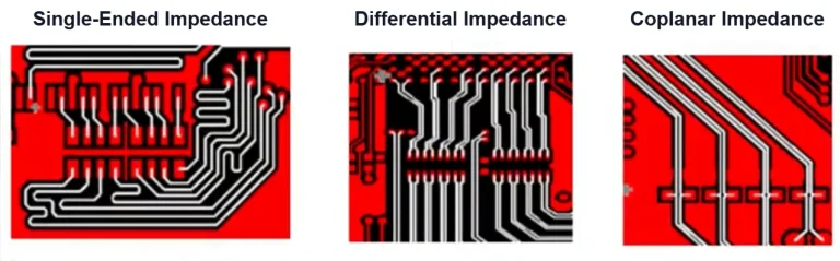
| Impedance control | ±8% on production runs; ±5% on prototype and special-review builds, single-ended and differential | Will you supply a TDR impedance test report with every batch? |
| Copper weight and hole processes | Heavy copper to 12 oz on samples and small batches; mechanical drilling to 0.15 mm finished holes, laser drilling to 0.1 mm | Are heavy copper and backdrill routine production processes for you, or special approvals? |
Use the benchmarks as conversation anchors, not as pass/fail gates — individual shops genuinely differ, and a supplier who answers with engineering context (yield at that trace class, which laminates they hold in stock, how the coupon is designed) is telling you something more valuable than a yes. For workmanship, an independent yardstick helps: the acceptance classes in IPC-A-600 and IPC-6012, published by the Global Electronics Association, let you specify class 2 or class 3 criteria instead of arguing over opinion. A structured walkthrough of layer counts, drill classes and inspection — the same benchmarks in production context — is on our multilayer PCB manufacturing capability page.
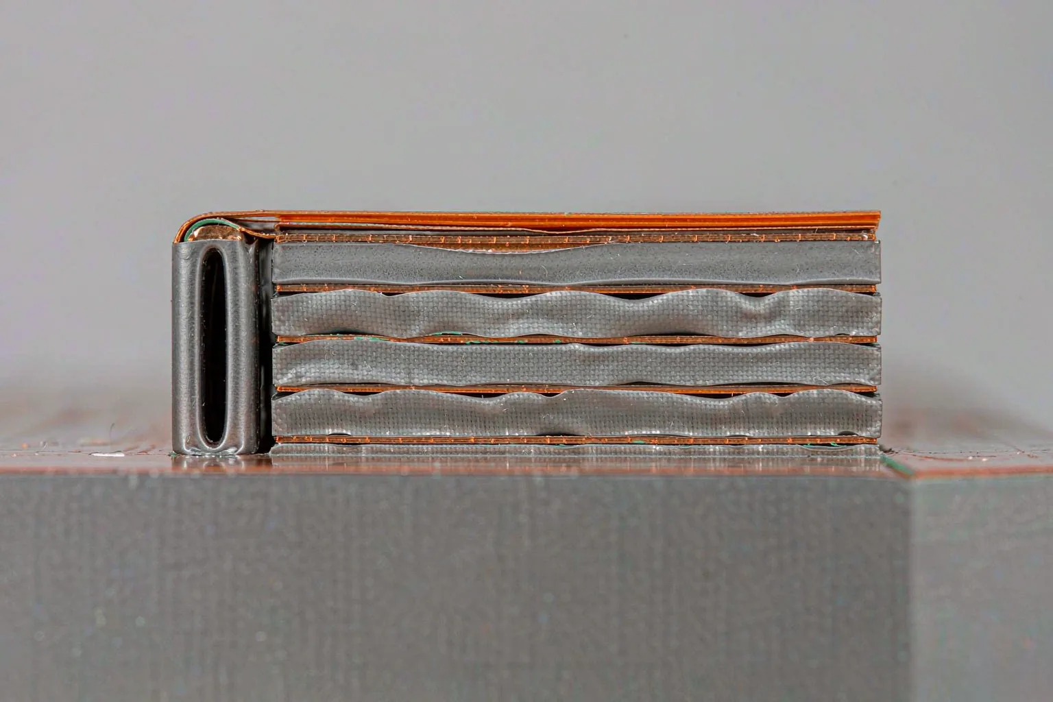
Prototype-to-Production Lead Times: Get the Numbers in Writing
The most common failure mode in multilayer sourcing is the gap between prototype and production: the samples arrive on time, the production order slips by two weeks, and nobody flagged the capacity conflict. Lead-time capability is therefore a selection criterion, not a logistics detail. Reference ranges for standard multilayer prototype builds look like this:
| Layer count | Expedited prototype | Standard prototype |
|---|---|---|
| 4 layers | 2 days | 5 days |
| 6 layers | 3 days | 7 days |
| 8 layers | 3 days | 9 days |
| 10–12 layers | 4–5 days | 11–12 days |
Treat these as reference ranges to be confirmed at engineering review, not as promises — HDI builds and special processes are quoted by tier, and an expedited 4-layer standard build shipping in as fast as 48 hours is a reasonable benchmark for a quick-turn line. The production side matters more: ask how a post-prototype order is scheduled, what happens to the slot if the trial batch finds an issue, and whether the engineering parameters from prototyping carry into production planning. Volume capacity is worth one question too — a group with three manufacturing plants and on the order of 3,000,000 m² annual capacity has surge headroom that a single-line shop does not, but only if you ask how your order routes through it.
Lead time and cost are linked, and both trace to the same few drivers. Before you compare quotes, it helps to understand what actually moves the price of a multilayer build — our breakdown of 4-layer PCB cost drivers covers the levers that show up again at every layer count.
Certifications and Outgoing Inspection: Two Documents to Collect
System certification is the entry ticket, and the floor is ISO 9001:2015. Automotive orders add IATF 16949; export and safety-regulated applications call for UL recognition and RoHS/REACH compliance; Canadian market access is covered by cUL recognition. The verification step that matters: request the certificate copies with their scope statements, and check that the scope actually covers PCB fabrication — a logo on a website verifies nothing, while a scope document tells you which site and which process the certificate covers.
Outgoing inspection is where a supplier either proves control or hides behind it. The routine configuration for a serious multilayer line is 100% electrical test, automated optical inspection (AOI), X-ray for BGA and via geometry, and TDR impedance testing on the coupon — with reports shipped with the goods. High-reliability orders add cross-section analysis and thermal stress verification on demand. If you want to read the reports a supplier sends, our guide to how TDR impedance measurement works explains what the numbers mean. Certificate authenticity can be checked at the UL Solutions certification database rather than taken from a brochure.
Then write both into the purchase contract: the certificates required, the test reports that ship with each batch, and the delivery window. Verbal commitments are the first thing to disappear when a line is under pressure — a one-page contract annex costs nothing now and settles every dispute later.
The RFQ Package: Send It Complete, Once
A fragmented RFQ costs you a full round trip per missing item, and each round trip adds a day to the decision. Send the package complete the first time:
- Gerber data in RS-274-X format (ODB++ is equally acceptable to most fabricators)
- Layer count and stackup requirements, including any controlled-impedance targets
- Laminate class — standard FR-4, higher-Tg, or a specified material system
- Surface finish (ENIG, HASL, OSP, and so on)
- Copper weight per layer, especially if any layer exceeds 1 oz
- Quantity split between prototype and production, and required delivery dates
- Special processes to be quoted: heavy copper, blind/buried vias, backdrill, edge plating
With complete data, a formal quote within 24 hours of engineering review is a normal commitment to expect — and the quote itself is diagnostic. A quote returned with no engineering questions asked is a warning sign, not good service: it means nobody checked whether your stackup is buildable as drawn. For the price structure behind the numbers, our article on how PCB pricing per square meter is built explains what the quote is actually composed of.
Validate with a Small Trial Order Before Production
There is a low-cost way to verify everything above without a factory visit: release the same Gerber package as a small trial order to two or three shortlisted suppliers, then compare the results side by side — sample consistency against the stackup, impedance coupon values against your targets, report completeness, and actual delivery against the promised date. The trial batch costs a fraction of what a failed production run costs, and it converts every claim in this checklist into an observation.
One deliberate outcome of the trial is consolidation. Keeping prototype and production with the same shop means the stackup parameters, impedance compensation values and engineering archive transfer automatically — no re-review, no re-learning of your design intent. The trial order validates the shop first; the production award then follows the evidence.
Red Flags When Screening a Multilayer PCB Manufacturer
The checklist above finds capability. Equally important is recognizing its absence early, because certain responses predict production trouble with unsettling reliability. Each item below maps directly to a later failure mode:
- Certification claims without scope documents — the certificate may cover a different site or a different process than the one building your boards
- A quote returned with no engineering questions — nobody reviewed the stackup, so the risk transfers to your production schedule
- No stackup proposal for a 10+ layer build — impedance and lamination planning were never done
- No TDR reports, or reluctance to provide per-batch data — outgoing inspection may not exist as a process, only as a claim
- Layer-count claims with no comparable shipped references — the number may describe capability that was demonstrated once, years ago
None of these flags is fatal by itself. Two or more together are a pattern, and patterns survive the sales conversation only to reappear in production. When you see one, ask the corresponding evidence question and watch what happens to the answer.
Matching Board Tier to Supplier Evidence
The checklist compresses into one rule: match the tier of your board to the tier of evidence you demand. An entry-tier 4–8 layer build needs a supplier with stable series production and consistent reporting — our 4-layer automotive PCB is representative of that class, where batch consistency and certified process control matter more than exotic capability. An advanced-tier build with impedance targets and higher layer counts needs the stackup proposal, the TDR regime and the shipped references checked explicitly — our 10-layer 2-stage HDI prototype illustrates the class of build where those checks are not optional.
Work the checklist in order and the supplier field sorts itself: the tier ranking eliminates shops that cannot build your board, the process questions eliminate shops that build it badly, the lead-time and certification checks eliminate shops that cannot hold commitments, and the trial order confirms the survivor. What remains is not a list of names — it is a shortlist with evidence attached.
Frequently Asked Questions
What types of multilayer PCB manufacturers are there?
By capacity profile, three groups: quick-turn prototype shops optimized for speed, comprehensive fabricators covering prototype through mid-volume production, and high-volume producers focused on series output. Our own footprint covers production of 2–30 layers with prototype builds to 64 layers per engineering review, and fast lines for both prototype and small-batch work. Match the group to your volume stage rather than assuming one shop type fits all.
How do I verify a multilayer PCB manufacturer’s layer capability?
Ask for shipped production references at your layer count and a stackup proposal for your specific design — not the number on the website. For 10+ layer boards, heavy copper, or blind/buried constructions, run a prototype first to verify lamination consistency and layer-to-layer registration before discussing production volumes.
How long does multilayer PCB prototyping take?
Reference ranges for standard builds: 4-layer prototypes ship in 2 days expedited or 5 days standard; 6 layers in 3/7 days; 8 layers in 3/9 days; 10–12 layers in 4–5/11–12 days. An expedited 4-layer standard build can ship in as fast as 48 hours. HDI and special-process builds are quoted by tier, so confirm the actual window at engineering review.
What impedance tolerance can I request on a multilayer board?
The common industry commitment is ±8% on production runs and ±5% on prototype or special-review builds, for both single-ended and differential pairs. Request a TDR impedance test report with every batch and keep the reports on file — tolerance claims without per-batch data are difficult to enforce after shipment.
What should I include in a multilayer PCB RFQ?
Gerber data in RS-274-X format, layer count and stackup requirements, laminate class, surface finish, copper weight, the prototype/production quantity split, and required delivery dates. A complete package lets engineering review finish in one pass, and a formal quote within 24 hours is a normal commitment to expect from an organized fabricator.
What outgoing tests should a multilayer PCB supplier run?
The routine set is 100% electrical test, AOI, X-ray inspection and TDR impedance testing on the coupon, with reports provided with the shipment. Orders with higher reliability requirements add cross-section analysis and thermal stress verification. Ask which tests are standard and which are optional before placing the order, and put the answer in the contract.
Why keep prototype and production with the same manufacturer?
Stackup parameters, impedance compensation values and the engineering archive transfer automatically when prototype and production run in the same shop — no re-review, no re-learning of design intent, and no second selection process. Validate the shop with a small trial batch first, then consolidate production with the supplier the evidence supports.
Get Your Stackup Reviewed Before You Commit
Instead of comparing names, put your Gerber in front of the engineering team: we review stackup, impedance targets and drill data before quoting, with multilayer production from 2 to 30 layers and prototype builds to 64 layers per engineering review.
Send your files through our PCB manufacturing services page and you will receive engineering feedback together with a detailed quote — the same review process this checklist asks of any supplier.