Book Appointment Now

A buyer's guide to portable SSD PCB design: an example 10-layer stackup, signal integrity rules, gold finger requirements and what to confirm before quoting.
Portable SSD PCB: Proven 10-Layer Stackup and Gold Finger Rules
A portable drive is the most physically punished product in consumer storage: it gets pocketed, dropped, run hot inside a sealed enclosure, and expected to move gigabytes over a single cable without a fan. The portable SSD PCB inside that enclosure has to pack a controller, NAND flash, power conversion and a USB or NVMe bridge onto a small rigid board, often thinner than 1 mm. It must also keep 6-16 Gbps differential pairs within tolerance. Desktop storage boards never face this combination of constraints.
This guide walks through the two build families inside portable drives and an example 10-layer portable SSD PCB stackup with real process parameters. It then covers the signal and power integrity rules that matter at these data rates. The manufacturing details follow – resin-plugged vias, gold fingers, warpage control – because they separate a reliable storage board from a warranty return. Use it as a checklist before you send a stackup out for quotation.
Table of Contents
- What Is a Portable Drive PCB?
- Bridge Board vs SSD Carrier: Two Very Different Builds
- An Example 10-Layer Portable SSD PCB Build
- Signal Integrity Rules for 6-16 Gbps Links
- Power Integrity and Heat in a Sealed Enclosure
- Gold Fingers: Thickness, Bevel and Insertion Life
- Manufacturing and Quality Controls That Matter for Storage Boards
- Prototype and Production Lead Times, Without the Guesswork
- Portable SSD PCB Quote Checklist
- FAQ
- Send Your Gerber for a Storage-Board Engineering Review
What Is a Portable Drive PCB?
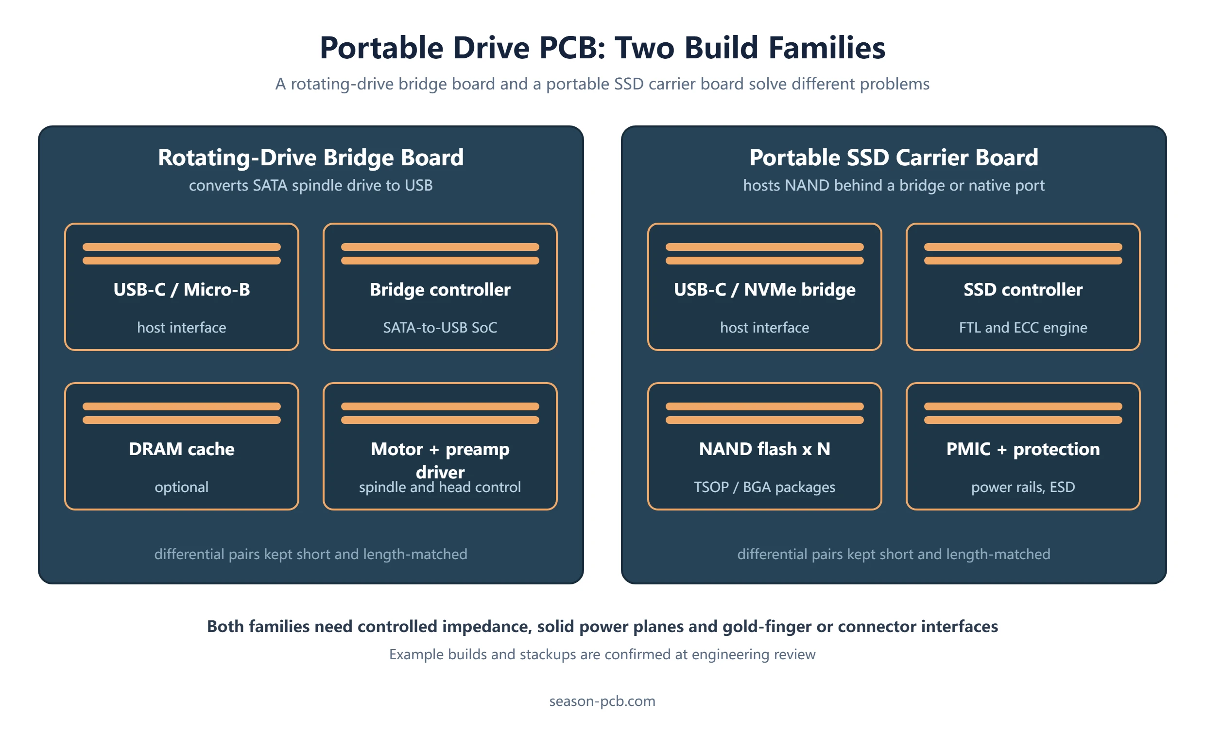
The term covers two quite different boards. In a rotating portable hard drive, the PCB is a bridge board: a modest 4-6 layer board. It converts the SATA spindle interface to USB, drives the motor and head preamp, and provides a small DRAM cache. Electrical demands are moderate, but the board must survive shock and vibration transmitted through the enclosure. The portable SSD PCB discussed next is a different class of build.
In a portable SSD, the PCB is a true carrier board: a high-layer-count board. It hosts the SSD controller, multiple NAND packages, power management and a USB-C or NVMe bridge, all within a footprint the size of a few NAND packages combined. Signal rates run from 6 Gbps (SATA class) up to 16 Gbps and beyond (NVMe-over-bridge class), so impedance control, length matching and reference-plane discipline are mandatory rather than optional. Those three rules are the backbone of any portable SSD PCB design review. This article focuses on the SSD carrier side, with the bridge board as a comparison point throughout. For a deeper treatment of the SSD-specific design decisions, see our SSD PCB design guide.
Bridge Board vs SSD Carrier: Two Very Different Builds
Sourcing teams sometimes quote both families as one line item and get surprised by the price gap. The table below shows why they are effectively different products from a manufacturing standpoint.
| Dimension | Rotating-drive bridge board | Portable SSD carrier board |
|---|---|---|
| Typical layer count | 4-6 layers | 8-12 layers |
| Signal class | 480 Mbps to 6 Gbps | 6-16 Gbps differential |
| Length matching | About ±10 mil | About ±5 mil or tighter |
| Material | Standard FR-4 | Mid-loss to low-loss laminate |
| Special processes | Usually none | Resin plugging, controlled impedance, beveled gold fingers |
| Relative cost factor | 1.0 (baseline) | Roughly 1.3-1.6x the baseline |
The cost factor is relative, not absolute – actual pricing depends on layer count, surface finish and volume – but the multiplier holds as a planning heuristic. If your product roadmap includes both form factors, qualify them as separate builds with separate stackups rather than forcing one design to serve both. The gap also explains why a portable SSD PCB is quoted as its own build, with a separate stackup.
An Example 10-Layer Portable SSD PCB Build
The specification below is a real-world example of a production portable SSD PCB build – the kind of stackup a mainstream 10 Gbps-class portable drive uses. It is useful as a calibration point when reviewing your own design, because every number below comes from a real portable SSD PCB build.
| Parameter | Example build | Why it matters |
|---|---|---|
| Layer count | 10 layers | Dedicated ground references for each high-speed pair group |
| Base material | FR-4 grade, Tg 170 | Thermal margin for sealed-enclosure operation |
| Finished thickness | 1.0 mm | Fits slim enclosure; thin enough for thermal transfer |
| Outer copper | 1 oz | Current handling and heat spreading |
| Inner copper | 0.5 oz | Fine-line inner routing with controlled impedance |
| Minimum via | 0.20 mm mechanical | Reliable drilling at production yield |
| Line/space | 3/3 mil | Escape routing under fine-pitch controller and NAND |
| Special process | Resin plugging | Via-in-pad escapes and planar surface for small packages |
| Surface finish | ENIG, 0.05-0.1 um gold | Flat, solderable pads for fine-pitch parts; connector fingers take a separate hard-gold finish |
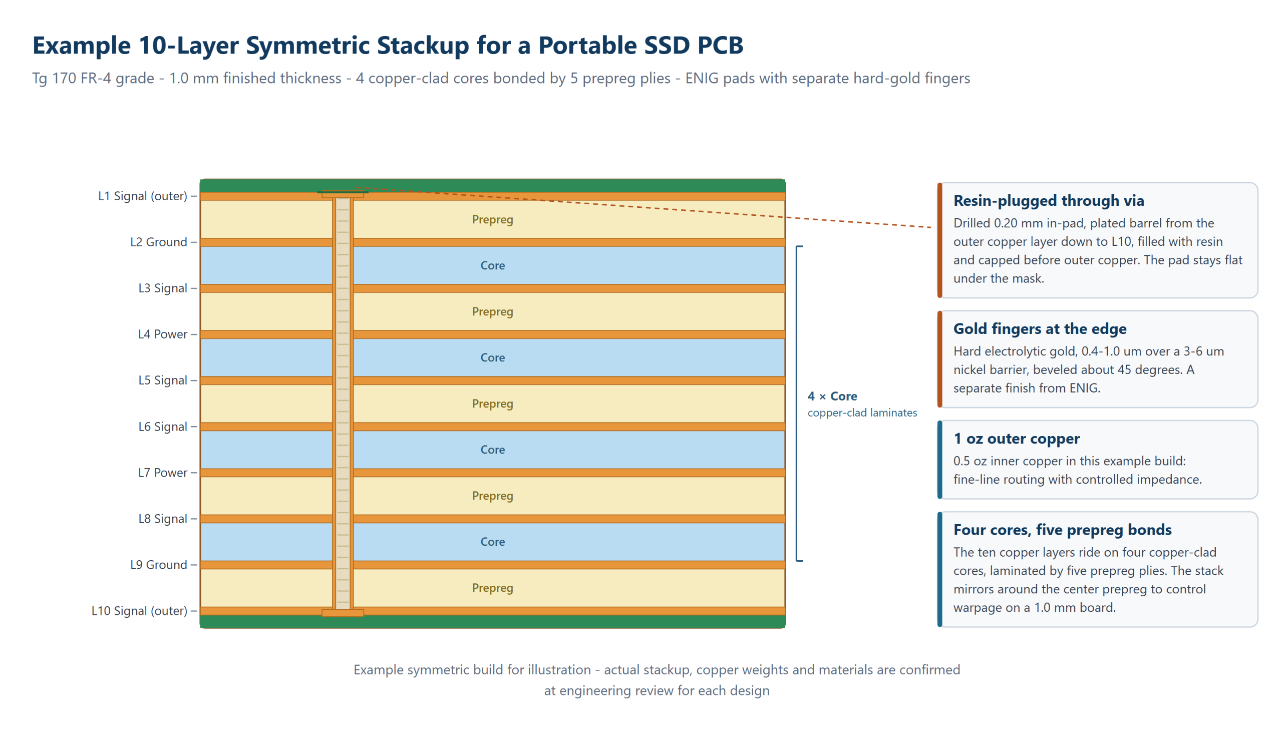
Three choices deserve explanation. First, resin plugging pairs with via-in-pad escapes: the controller’s fine pitch leaves no room for dogbone escapes on every ball, so vias are drilled in-pad, filled with resin and capped before outer copper. Second, the symmetric 10-layer stack mirrors copper and dielectric around the center core – on a 1.0 mm board, symmetry is the primary warpage defense. Third, ENIG gives the flat, solderable pads that fine-pitch packages need. The edge connector fingers get a separate finish – hard gold, not ENIG. If your build is an M.2 module instead of a USB drive, our 10-layer M.2 SSD PCB page shows the connector-driven variant of this stackup.
Signal Integrity Rules for 6-16 Gbps Links
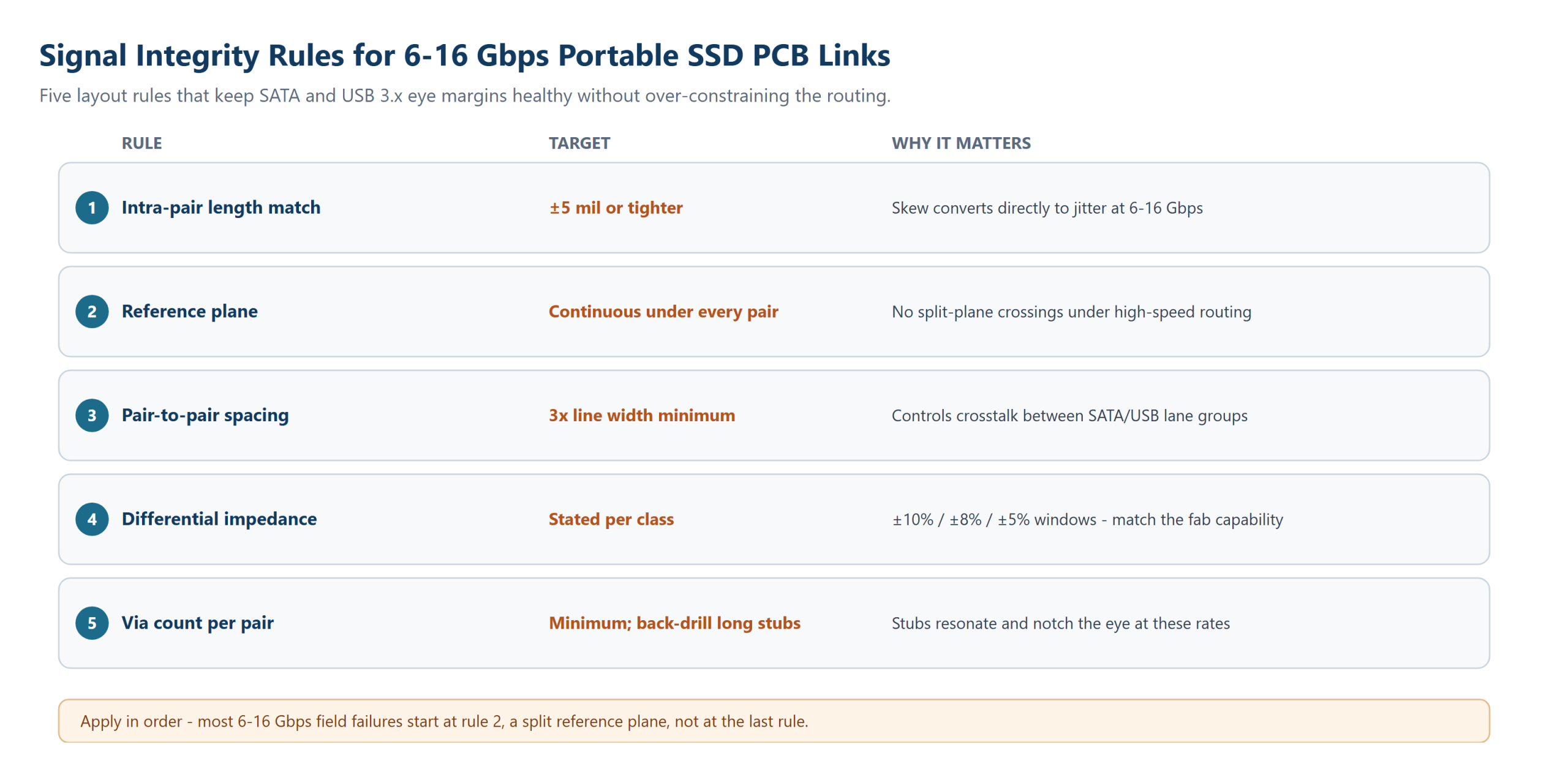
At SATA and USB 3.x data rates, a storage link fails quietly: the drive passes bench tests but drops transfers when the enclosure warms up or the cable is marginal. The design rules below keep eye margins healthy without over-constraining the layout. Apply them in order: a portable SSD PCB usually fails at the first split reference, not at the last rule.
| Rule | Target | Rationale |
|---|---|---|
| Intra-pair length match | ±5 mil or tighter | Skew converts directly to jitter at 6-16 Gbps |
| Reference plane | Continuous under every pair | No split-plane crossings under high-speed routing |
| Pair-to-pair spacing | 3x line width minimum | Controls crosstalk between SATA/USB lane groups |
| Differential impedance | Stated per class, ±10%/±8%/±5% windows | Tolerance must match the fab’s proven capability |
| Via count per pair | Minimum; back-drill if stubs exceed limits | Stubs resonate and notch the eye at these rates |
Two practical additions for any portable SSD PCB layout. Keep the NAND-to-controller fly-by or ring routing groups consistent – mixed topologies create per-byte-group timing spread that the controller must then tolerate. And reserve the inner layers adjacent to high-speed pairs exclusively for ground; a power plane is an acceptable reference only when it is stitched to ground around every signal crossing. Our signal trace design guide covers the routing mechanics in depth.
Power Integrity and Heat in a Sealed Enclosure
An SSD controller bursts to several amps when writing sustained SLC-cache streams, and it draws that current from a single USB-C 5 V rail through onboard conversion. The PDN – power distribution network – has to present low impedance from DC through the controller’s burst frequency, or the rail sags mid-write and the drive glitches. Wide power planes, one bulk capacitor per rail cluster and dense decoupling at each IC supply pin are the baseline; confirm the PDN with a target-impedance check rather than by eyeball. On a portable SSD PCB the 5 V rail is also the rail the host can throttle, so PDN margin is a user-visible specification.
Thermally, the enclosure is the problem. A sealed aluminum or plastic shell turns the PCB into the main heat spreader, so 1 oz outer copper is not just electrical – it moves heat from the controller to the shell. Some designs add a thermal pad from the controller’s backside through to the enclosure wall. Keep hot zones – controller, PMIC – away from NAND, because sustained NAND temperature shortens data retention. These are stackup-level decisions: a redesign after thermal testing costs a full prototype cycle. Copper weight and thermal-via placement are the two cheapest levers a portable SSD PCB has.
Gold Fingers: Thickness, Bevel and Insertion Life
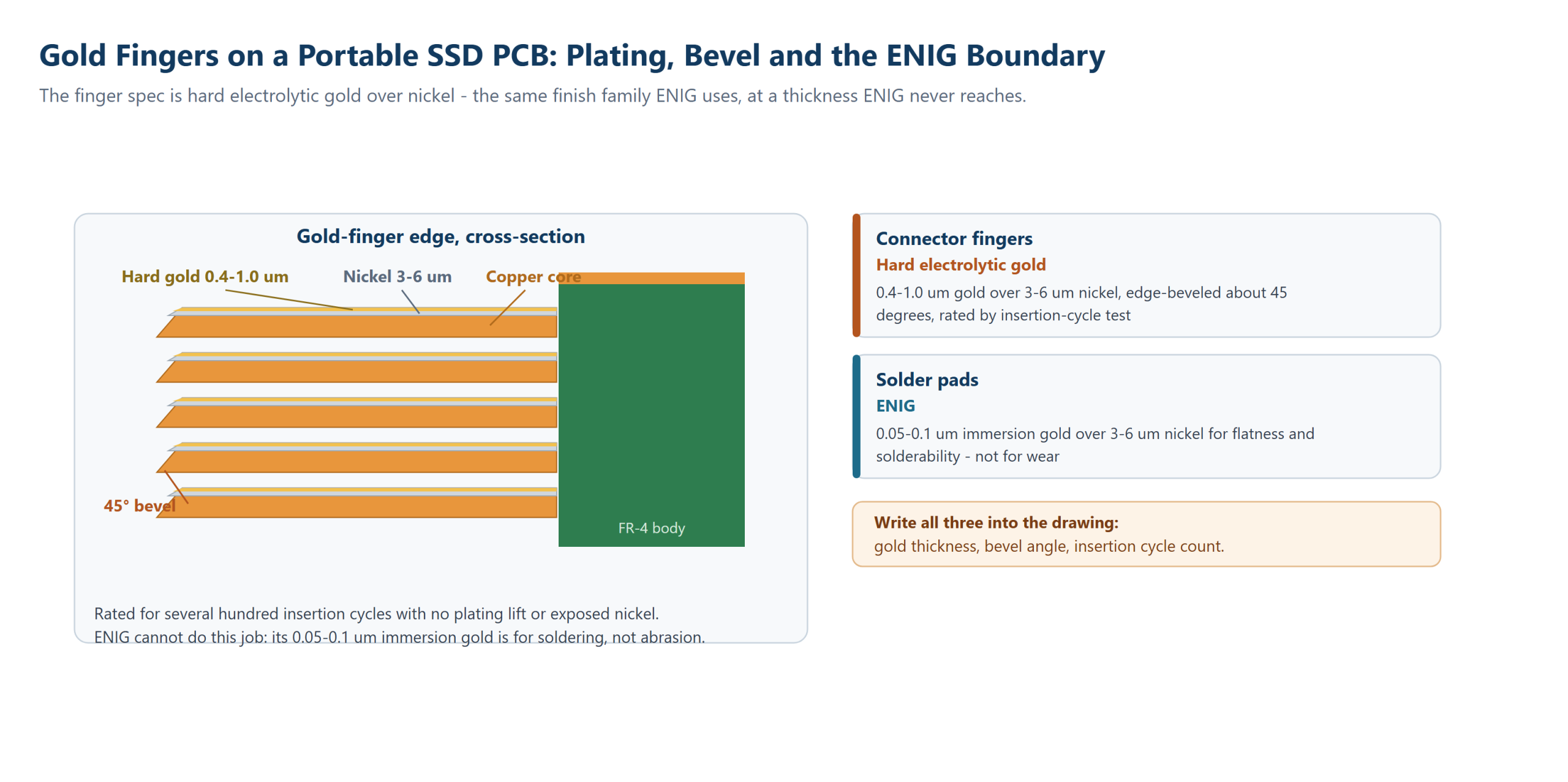
Portable drives live on their connectors, and no part of a portable SSD PCB works harder than the gold fingers. A USB stick, an M.2 module or a card-style portable SSD mates and unmates dozens of times over its life, and the gold fingers take every insertion. The specification that matters is hard gold (electrolytic nickel-gold) on the fingers – not ENIG, which is designed for soldering, not abrasion. Hard gold plating over nickel resists wear; typical builds target a gold thickness in the 0.4-1.0 um range with the nickel barrier underneath.
Beveling is the second half of the spec, and the half most portable SSD PCB drawings leave out. Fingers are edge-beveled at roughly 45 degrees so the lead-in does not scrape the connector socket, which prevents both gold smear and socket damage. An insertion-and-extraction cycle test – several hundred mates with no plating lift or exposed nickel – is a reasonable factory acceptance criterion to write into your drawing. Specify the finger chamfer, gold thickness and cycle count explicitly; left unspecified, fingers default to whatever the fab’s standard flow produces.
Manufacturing and Quality Controls That Matter for Storage Boards
Storage carrier boards earn their keep in the field, so the quality controls to insist on are the ones that predict field behavior. AOI on all copper layers catches fine-line defects before lamination makes them invisible. That first look matters most on a portable SSD PCB, where 3/3 mil traces leave little margin for rework. Electrical test – flying probe for prototypes, test fixtures in production – verifies every net 100%. First-article cross-sections confirm via fill quality, plating thickness and layer alignment; on a resin-plugged build, the cross-section is the only way to verify the fill actually reached specification.
Warpage is the quiet killer on thin portable SSD PCB builds. A 1.0 mm board that ships flat can bow during reflow and mis-register in the enclosure or connector. IPC-6012-class flatness (0.75% of board length) is the working criterion, and symmetric stackup plus flatness inspection before shipment is how it is achieved. Impedance test reports per production batch, with coupon data archived, close the loop between the stackup you approved and the boards you receive.
Prototype and Production Lead Times, Without the Guesswork
A 10-layer resin-plugged portable SSD PCB is a mid-complexity build: not a commodity 4-layer, not a 3-stage HDI exotic. Realistic planning windows are typically 5-7 working days for prototype quantities and 15-20 working days for volume production. The confirmed schedule is issued at engineering review, because the actual number depends on stackup specifics, material availability and current queue depth, not on a published table.
Two schedule protectors for a portable SSD PCB order. First, complete the stackup and impedance targets before RFQ: re-quotes after engineering feedback are the most common self-inflicted delay. Second, flag special processes – resin plugging, hard-gold fingers, beveling – in the initial package so the fab quotes them into the schedule instead of discovering them after order placement. Annual group capacity here is 3,000,000 m2 across three sites, which matters for the production ramp, not the prototype week.
Portable SSD PCB Quote Checklist
A complete portable SSD PCB RFQ package gets a firm quote and a real engineering review in the first pass. Before submitting, confirm you have covered:
- Gerber or ODB++ data including drill files, with the stackup intent noted per layer.
- Impedance targets per signal class, with tolerance windows stated.
- Special processes: resin plugging (with which vias), hard-gold fingers, bevel angle.
- Finished thickness and warpage criterion, especially below 1.0 mm.
- Surface finish per zone – ENIG for pads, hard gold for fingers.
- Volume split: prototype quantity, pilot, and expected annual production.
- Enclosure constraints that affect board outline, mounting holes or thermal interface.
For reference builds, our 10-layer portable SSD PCB and 4-layer SATA SSD PCB product pages show two calibrated points on the complexity ladder. When you are ready to submit, the Gerber format itself is documented by its maintainer at Ucamco, and the IPC standards library remains the reference for design and acceptance criteria.
Frequently Asked Questions
What is a portable SSD PCB?
It is the carrier board inside a portable solid-state drive. It hosts the SSD controller, NAND flash packages, power management and a USB or NVMe bridge on a compact rigid board, typically 8-12 layers and around 1.0 mm thick. It runs 6-16 Gbps differential links, so impedance control, length matching and resin-plugged via-in-pad escapes are standard manufacturing requirements.
Can the same factory build HDD bridge boards and SSD carrier boards?
Usually yes, but they are different products. A rotating-drive bridge board is a 4-6 layer board with moderate signal rates, while a portable SSD carrier needs 8-12 layers, controlled impedance, resin plugging and hard-gold fingers. Quote them as separate builds – forcing one stackup to serve both wastes money on one and under-specifies the other.
Why do portable drive PCBs use resin-plugged vias?
On a portable SSD PCB, the controller and NAND packages have fine pitch that leaves no routing room for dogbone via escapes on every ball. Placing vias directly in the pads with resin fill and capping creates a planar, solderable surface and short escape paths. The fill also prevents solder wicking into the via during assembly, which would starve the joint.
What gold finger specifications do storage drive PCBs need?
Specify hard electrolytic gold over a nickel barrier on the fingers, typically 0.4-1.0 um of gold over 3-6 um of nickel, with edge beveling at about 45 degrees. ENIG is for solderable pads, not for insertion wear. A reasonable acceptance test is several hundred insertion cycles with no plating lift or exposed nickel.
How thin can a portable SSD PCB be?
Production builds commonly run around 1.0 mm, and thinner builds are possible with symmetric stackup design and Tg 170-class FR-4 to control lamination stress. The binding constraint is usually warpage: IPC-6012-class flatness of 0.75% of board length must hold through reflow and enclosure assembly, so confirm the thickness target with your fabricator before finalizing the mechanical design.
What files do I need for a portable SSD PCB quote?
For a portable SSD PCB RFQ, supply Gerber or ODB++ data including drill files, plus the intended stackup with impedance targets and tolerance windows. Add a clear list of special processes – resin plugging locations, hard-gold fingers with bevel angle, finished thickness and warpage criterion. A complete package gets a firm, reviewable quote in the first pass instead of a re-quote cycle.
How long does a portable drive PCB prototype take?
A 10-layer resin-plugged storage build typically takes 5-7 working days for prototypes and 15-20 working days for volume production, with the confirmed schedule issued at engineering review. Flag special processes in the initial RFQ – they affect both cost and schedule and are the most common cause of re-quoting delays.
Send Your Gerber for a Storage-Board Engineering Review
If your portable SSD PCB design is heading to prototype, send the Gerber package and stackup intent for an engineering review before you commit. We will check the impedance targets against the routing classes and confirm the resin-plugging and gold-finger specifications. You then get a firm lead time with the quote, so the schedule you plan around is the schedule you get.
Season Multilayer Circuit manufactures 2-30 layer rigid PCBs for storage, automotive, industrial and consumer applications as part of the 998 PCB Group, with 3,000,000 m2 of annual group capacity. Browse more application guides in our PCB basics library or review the full PCB manufacturing services scope.
Get Your Portable SSD PCB Build Reviewed Before You Commit
If the build described above is close to your design, send the stackup intention and Gerber data for engineering review. We return feasibility comments on layer count, via structure and panel efficiency, plus the production detail behind the 10-layer M.2 SSD PCB in this article. Anything outside standard process windows is flagged with the cost and lead-time deltas attached, before you commit a layout.