Book Appointment Now

A buyer's guide to the 4-layer router PCB: reference stackup, 50 ohm layout rules, resin plugging, material alternatives and lead times for volume.
4-Layer Router PCB: Stackup, RF Layout and Material Choice
A 4-layer router PCB has to do three jobs at once: break out a dense SoC, keep several radios from interfering with each other, and stay cheap enough for a consumer price point. Most router main-board failures we see at DFM review are not exotic; they are 2-layer boards stretched past their limits, or RF feeds whose reference plane was broken by a split nobody noticed until certification.
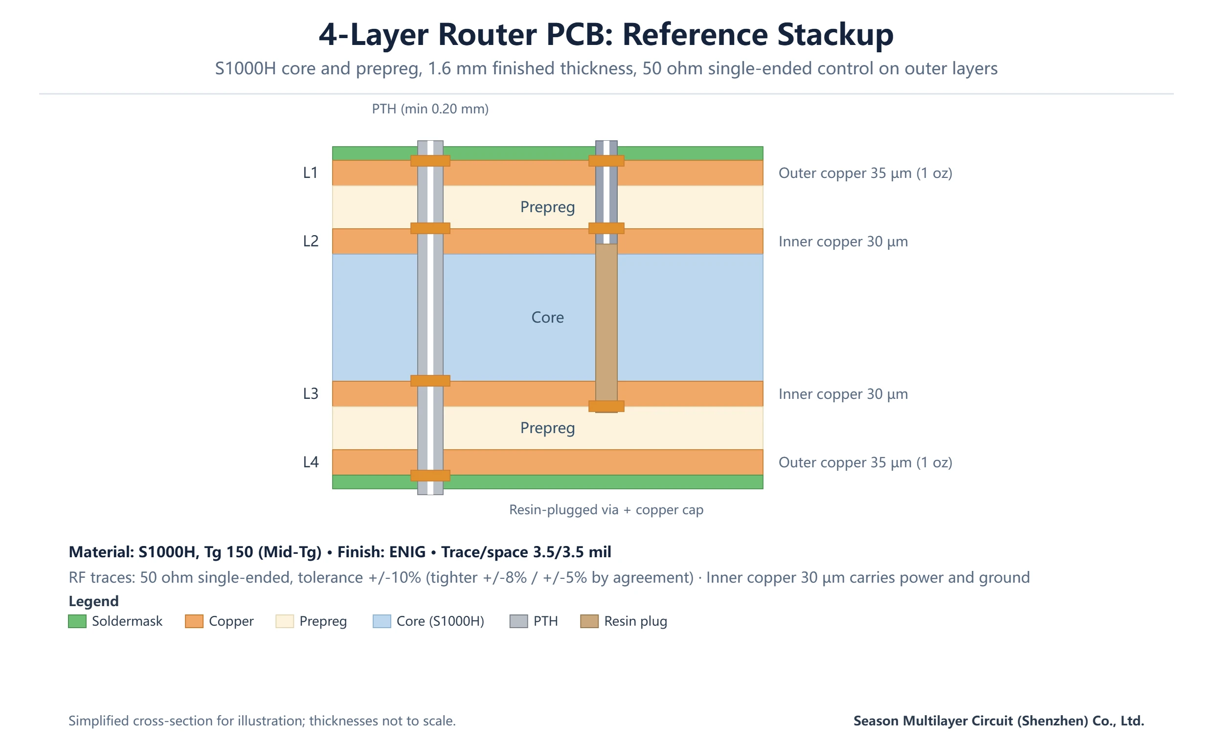
This guide walks through the reference build we produce for router and gateway main boards: a 4-layer stackup on S1000H laminate (Tg 150, Mid-Tg), 1.6 mm finished thickness, 35 µm outer and 30 µm inner copper, ENIG finish, with resin-plugged vias in the high-density zones. You get the full specification table, a comparison against 2-layer boards, the RF layout rules that survive certification testing, and the material alternatives when the program outgrows the reference grade.
Table of Contents
- What Is a 4-Layer Router PCB?
- 4-Layer Router PCB Stackup and Specifications
- Why Four Layers Beat a 2-Layer Board in a Router
- RF Layout: 50 Ohm Control and Antenna Isolation
- Resin-Plugged Vias: Where They Earn Their Keep
- Router PCB Design Rules and DFM Checklist
- Testing and Quality Control
- Material Choices: When to Look Beyond the Reference Grade
- Lead Times and Scaling to Volume
- FAQ
- Get Your Router Stackup Reviewed Before You Release Gerber
What Is a 4-Layer Router PCB?
A 4-layer router PCB is the main board of a home or small-office router, gateway or mesh node. It carries the network SoC, RAM and flash, an Ethernet PHY section, a Wi-Fi front end with its antennas, and a power section fed from a 12 V adapter. The same construction family covers set-top boxes, access points and smart-home hubs, which is why the stackup below repeats across a whole product category.
Four copper layers are the practical entry point for anything with a radio. Two layers cannot give both the digital section and the RF front end an unbroken reference plane, and without one, the 50 ohm feedlines and the Ethernet magnetics lose the ground the design depends on. Our 4-layer router PCB product page lists this build as a standard offering, and the figures in this article match it exactly.
For buyers, the interesting boundaries are these: below four layers, radio certification becomes a layout gamble; above six layers, you are usually looking at multi-band Wi-Fi 6/7 platforms with more PHYs than a 4-layer build can place. Between those poles, the 4-layer stackup is the cost-quality sweet spot that most consumer networking hardware lands on.
4-Layer Router PCB Stackup and Specifications
The reference stackup is deliberately boring: two prepreg-bonded copper pairs around an S1000H core, symmetric top to bottom. S1000H is a Tg 150 mid-Tg FR-4 grade that balances cost, drillability and stable dielectric behaviour at router frequencies. The parameters below are the ones quoted on the product page.
| Parameter | Reference value |
|---|---|
| Layer count | 4 layers |
| Base material | S1000H, Tg 150 (Mid-Tg) |
| Finished thickness | 1.6 mm |
| Outer copper | 35 µm (1 oz) |
| Inner copper | 30 µm |
| Minimum via | 0.20 mm mechanical |
| Trace / space | 3.5 / 3.5 mil |
| Surface finish | ENIG |
| Special process | Resin plugging in high-density zones |
| Reference panel | 156 × 114 mm panel, 2 boards up |
Two choices in this table do real work. The 30 µm inner copper is heavier than the usual 18 µm: it lowers the ground impedance that both the RF returns and the Ethernet pairs reference, and it carries the 12 V input rail with less voltage sag. And ENIG gives the flat, oxidation-resistant pads that fine-pitch SoCs and press-fit shield cans need across a long shelf life.
Why Four Layers Beat a 2-Layer Board in a Router
A 2-layer board can run a simple 2.4 GHz-only node if the layout is disciplined. Add a 5 GHz radio, gigabit Ethernet or more than one antenna, and the two-layer construction starts consuming engineering time that costs more than the board saves. The table shows where the difference actually lands.
| Dimension | 4-layer router PCB | 2-layer board |
|---|---|---|
| Reference planes | Dedicated ground on L2 for RF and Ethernet | Shared, frequently split |
| RF feed control | 50 ohm single-ended, tolerance ±10% | Impedance uncontrolled |
| Fine-pitch SoC | 0.25 mm pitch escapes comfortably | Fan-out congests quickly |
| EMC behaviour | Clean returns; certification rework rare | Frequent iteration on shields and filters |
| Relative cost factor | Roughly 1.6–2.2× | 1.0× |
The cost multiplier is relative, not a quote: yield and panel utilisation move it in both directions. The honest comparison is total program cost. On a 4-layer build, certification tends to pass on the first or second chamber run; on a stretched 2-layer board, each extra EMC iteration costs test-house fees and weeks of schedule, which is the expensive part, not the laminate.
RF Layout: 50 Ohm Control and Antenna Isolation
On the reference stackup, RF feeds run on L1 as 50 ohm single-ended lines with L2 as an unbroken ground beneath them. We hold the impedance to ±10% as standard, with ±8% or ±5% available by agreement when a radio module’s matching network needs the margin. Our impedance measurement guide explains how that is verified with coupons rather than assumed from the design file.
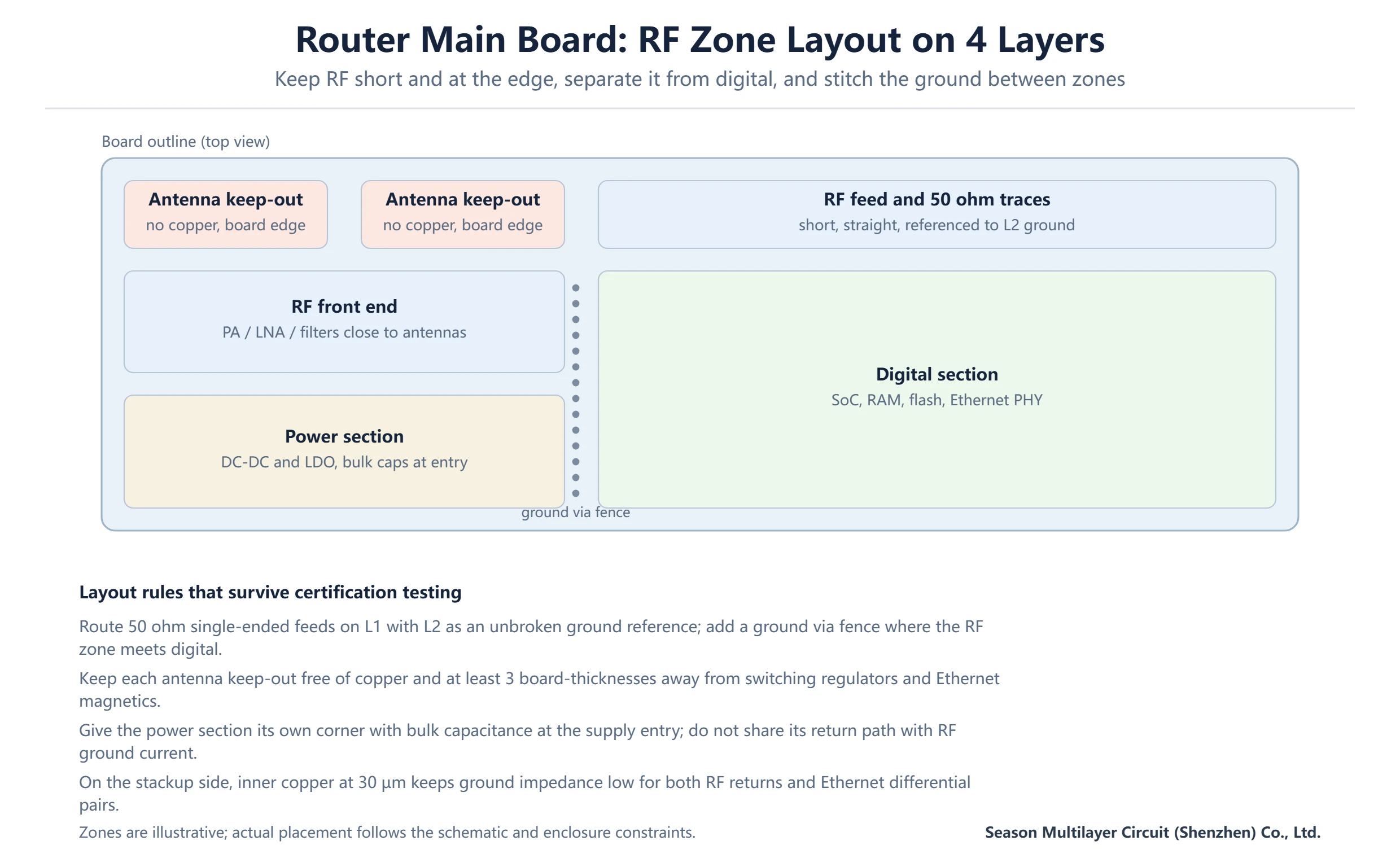
Zone discipline matters as much as trace geometry. Antennas live at the board edge with their keep-outs free of copper on every layer; the PA, LNA and filters sit close behind them; the SoC and Ethernet PHY are pushed to the digital corner; and the switching regulators keep their own ground corner at the supply entry. A fence of ground vias stitches L1 to L2 where the RF zone meets the digital zone, so return currents never have to detour.
The 30 µm inner copper earns its cost here too: a heavier ground plane keeps the return path impedance low for both the RF section and the gigabit pairs, and it damps the ground bounce that would otherwise couple radio noise into the Ethernet interface. Boards built this way pass coexistence and emissions testing with fewer shield revisions.
Resin-Plugged Vias: Where They Earn Their Keep
The reference build calls out resin plugging as its special process, and on a router main board it has two jobs. In the dense SoC fan-out area, vias drilled through the outer layers are filled with resin and capped with plated copper so that routing can pass over them and pads stay solid under the SoC. Along the RF section, plugged vias keep the ground stitching tidy without leaving barrels that shed solder onto nearby feed pads during reflow.
The process sequence is drill, plunge-plug with cured resin, grind flat, then cap with copper before the outer-layer pattern plating. Fill quality is verified by cross-section per lot; an underfilled plug shows up later as a dimpled pad or, worse, a void that outgasses during reflow. For a deeper comparison of plug materials and their trade-offs, see our guide to resin versus solder-mask ink plugging.
You do not need plugging everywhere. On the reference board it is confined to the zones that need it, which keeps the added process steps and their cost impact proportionate. If your layout can live with vias under packages left open, say so at review; unplugged barrels are cheaper and perfectly reliable when the design allows them.
Router PCB Design Rules and DFM Checklist
These are the checks our engineers run before any 4-layer router PCB panel is cut, and they are worth self-auditing before you release Gerber:
- Route every RF feed on L1 with an unbroken L2 ground beneath it; a split plane under a feedline shifts its impedance more than any etch tolerance does.
- Hold 3.5/3.5 mil trace and space as the outer-layer budget; finer rules push the board into narrower-process pricing.
- Keep each antenna keep-out clear of copper, including pour, on all four layers, and model the shield can before fixing antenna positions.
- Stitch a ground via fence where the RF zone borders the digital zone, and do not let digital returns share the RF ground path.
- Place bulk capacitance at the 12 V entry and give the regulators their own corner away from the antennas.
- Send the stackup with the Gerber package so copper balance, impedance and resin-plug zones are reviewed before lamination.
The PCB manufacturing services page lists what a DFM review covers, and on router projects it most often catches split reference planes and antenna keep-out violations, the two defects that are cheap to fix in CAD and expensive to fix in a certification chamber. If you want to sanity-check the layer stack itself, our stackup design guide walks through the balancing rules behind this construction.
Testing and Quality Control
Router boards hide their worst failure modes under shield cans and connectors, so inspection concentrates at the panel stage where every square millimetre is still visible. The reference flow combines 100% automated screening with per-lot sampling.
| Check | Method | What it catches |
|---|---|---|
| Outer-layer defects | AOI on every panel | Opens, shorts, 3.5 mil width violations |
| Electrical continuity | Flying probe or fixture test, 100% | Barrel voids and net opens invisible to AOI |
| Impedance | Coupon TDR per panel | Drift in 50 ohm RF feeds and pair geometries |
| Plug quality | Cross-section per lot | Underfilled resin, cap plating gaps |
| Final visual and thickness | Sample per panel | ENIG quality, soldermask coverage, 1.6 mm thickness |
Acceptance criteria reference IPC class 2 workmanship as standard, with class 3 available for infrastructure-grade products; the governing documents are indexed on the IPC standards page. First-article confirmation locks the process before volume, and engineering parameters are archived per batch so repeat orders match the approved sample, batch after batch.
Material Choices: When to Look Beyond the Reference Grade
The reference grade covers most cost-driven router builds: Tg 150 handles reflow and typical gateway ambient temperatures with margin, and its dielectric properties are stable enough for 2.4/5 GHz front ends whose critical impedances live in the layout, not the laminate. Moving up a material class buys little until the design pushes 5 GHz harmonics through long internal runs or the product targets elevated operating temperatures.
Two upgrades cover most of those cases. Where a program mandates halogen-free laminate, the S1150G grade (Tg 150 or higher) is the standard drop-in, and the stackup geometry carries over with only prepreg substitutions. Where radios move to higher bands or traces get electrically long, a hybrid stackup that keeps the digital section on FR-4 while placing a low-loss dielectric on the RF layers adds performance without repricing the whole board; our PCB materials and laminates guide compares the options and their typical use cases.
For completeness, 1.6 mm is the reference thickness because it matches off-the-shelf connectors, enclosure clips and RJ45 jack tolerances. Thinner or thicker builds are manufacturable, but they ripple through the mechanical BOM, so treat thickness as a system decision rather than a board-level one.
Lead Times and Scaling to Volume
For the reference 4-layer build, prototype runs complete in roughly 5–7 working days and volume runs in 15–20 working days, with the firm schedule confirmed at engineering review once the stackup and panel are locked. Complete Gerber and stackup data on day one is the single biggest schedule lever; missing plug-zone or impedance callouts are the usual causes of a slipped start.
Volume production scales across three group plants in Shenzhen, Jiangxi and Anhui with a combined 3,000,000 m² of annual capacity across 2–30 layer technologies. Router programs benefit twice from that footprint: seasonal peaks queue across a large capacity pool, and the 2-up reference panel can be re-optimised to higher board counts as the design stabilises, stepping unit cost down through the product life.
Repeat orders inherit the archived engineering parameters from the approved first article, so a batch shipped in month eighteen matches the sample your certification was based on. That traceability is what lets a networking brand keep a single qualification file per product rather than re-testing on every supplier change.
Frequently Asked Questions
Is a 4-layer board enough for a Wi-Fi 6 router?
For single-band and simultaneous dual-band Wi-Fi 6 platforms, yes: the reference 4-layer construction carries the SoC, PHYs and two radio chains with controlled-impedance feeds. Multi-band Wi-Fi 6E/7 designs with three radio chains and more front-end components usually move to 6 layers, mainly for escape routing and reference-plane flexibility rather than material performance.
Why is S1000H used on router main boards?
It is a Tg 150 mid-Tg FR-4 grade with stable dielectric behaviour at router frequencies, good drillability for 0.20 mm vias, and a cost position that fits consumer networking hardware. Its reflow and operating temperature margins cover typical gateway environments, which is why it is the default laminate in this category rather than a specialised high-frequency material.
What impedance tolerance can you hold on RF traces?
The standard commitment is ±10% on 50 ohm single-ended feeds, verified by coupon TDR per panel. Tighter windows of ±8% or ±5% are available by agreement when a radio module’s matching network needs the margin. The tolerance is measured on production coupons, not assumed from the design file, and results ship with the batch documentation.
Why is the inner copper 30 µm on this build?
The heavier-than-usual inner copper lowers the ground impedance that RF returns and gigabit Ethernet pairs reference, and it carries the 12 V input rail with less voltage sag across the board. On a router main board those two jobs sit on the same layers, so the extra copper buys both signal integrity and power distribution at once.
What is resin plugging used for on a router board?
In the SoC fan-out zone, plugged vias let routing cross over them while keeping pads solid during assembly. In the RF section they keep ground stitching tidy without open barrels that shed solder during reflow. Fill quality is verified by cross-section per lot. It is applied only where needed, since each plug adds process steps and cost.
What files should I send for a 4-layer router PCB quote?
A complete Gerber package including drill files, the stackup table, and a note of which nets are impedance-controlled and which vias are resin-plugged. Fabrication drawings are welcome but optional. With those files the DFM review returns concrete feedback on reference planes, antenna keep-outs, panel utilisation and any spec outside standard process windows.
How long do prototype and volume runs take?
Prototype runs for the reference 4-layer build complete in roughly 5–7 working days and volume in 15–20, confirmed at engineering review. The schedule assumes complete Gerber and stackup data on day one. Volume capacity draws on three group plants with 3,000,000 m² of annual capacity, so ramping a successful router program does not require requalification or a new supplier file.
Get Your Router Stackup Reviewed Before You Release Gerber
Send your Gerber and stackup for a free DFM review, and you will get back a concrete read on reference-plane integrity, antenna keep-outs, impedance control and resin-plug zones before the first panel is cut. The 4-layer router PCB product page lists the full reference specification and build options.