Book Appointment Now

Why AI server PCB builds run 20+ layers on very-low-loss laminate: stackup choices, via structures, impedance tolerances and the cost drivers behind the premium.
AI Server PCB: Layer Counts, Materials and Cost Drivers
Quotes for AI infrastructure boards look nothing like the quotes hardware teams are used to receiving for conventional server products. A board that would have been specified at 12 layers two years ago is now being drawn at 24, and the laminate line item alone can double the material share of the build. If you are sourcing an AI server PCB for the first time, the premium is easy to misread as margin when it is actually driven by physics and process time.
This guide breaks down what actually changes between a conventional server board and an AI server PCB: layer counts and stackup logic, laminate classes, via structures such as back-drilling and resin plugging, impedance tolerances, and the relative cost drivers behind the multiplier. The goal is to give engineers and buyers a shared vocabulary for the first engineering review, not a translation of a datasheet.
Table of Contents
- What Makes an AI Server PCB Different
- AI Server PCB Layer Counts and Stackup Logic
- AI Server PCB Materials: Why Loss Class Matters
- Via Structures: Back-Drilling, Resin Plugging and HDI
- Accelerator Carrier Boards Concentrate the Value
- Why an AI Server PCB Costs More
- Impedance Control and Testing on AI Builds
- Design Handoff Checklist Before You Request a Quote
- Choosing a Manufacturer for AI-Class Builds
- FAQ
- Get Your AI Server PCB Stackup Reviewed Before You Commit
What Makes an AI Server PCB Different
The term covers a family of boards inside AI compute clusters rather than one product: accelerator carrier boards that host GPU or ASIC modules, switch boards that route the fabric, line cards, midplanes and backplanes. What they share is an interconnect problem. Every accelerator module exchanges hundreds of high-speed serial lanes with its neighbours, and every one of those lanes has to arrive with an open eye at 32 GT/s and beyond.
A conventional server board is dominated by moderate-speed buses, storage interfaces and management traffic, so the design pressure sits on cost and power delivery. An AI server PCB shifts the pressure to signal integrity: the routing budget, the laminate loss, the via stubs and the impedance tolerances all tighten at once. That is why two boards with similar footprints can differ by a factor of several in build complexity.
For buyers, the practical consequence is that the Bill of Materials conversation starts with the stackup, not the board area. The stackup decisions determine which fabricators can even quote the job, and they drive most of the cost gap explained later in this guide.
AI Server PCB Layer Counts and Stackup Logic
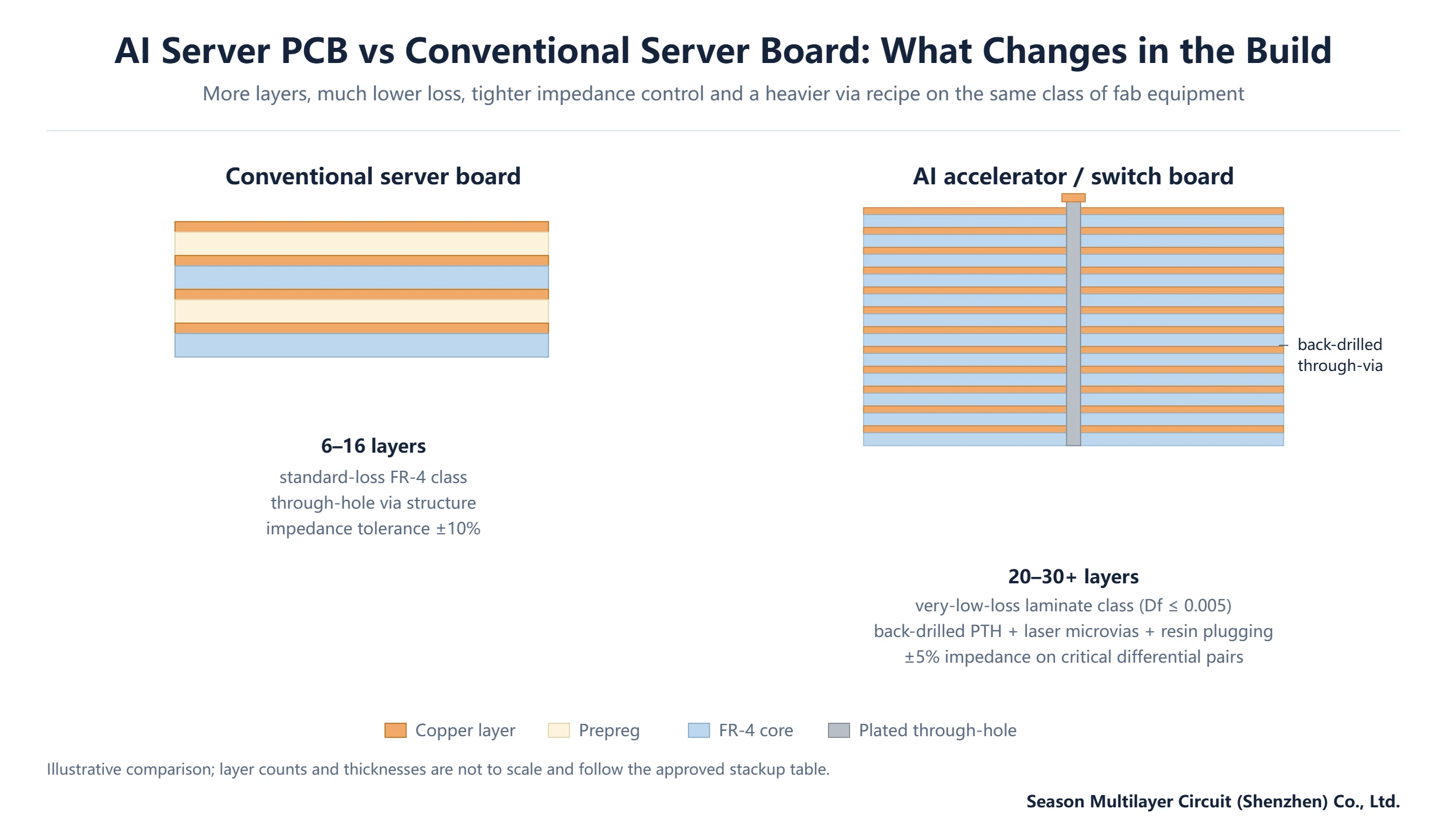
Conventional server motherboards typically land between 6 and 16 layers. Boards inside AI clusters routinely specify 20 to 30 layers, and switch fabric boards push higher still. The count is not a status symbol; it is the arithmetic of escape density. A large BGA with thousands of balls needs enough signal layers to break out every lane, plus enough uninterrupted reference planes to keep each lane’s return path solid.
More layers also mean more lamination cycles, more drilling steps and longer registration chains. Each press adds a chance for layer-to-layer misalignment, so a 24-layer build is not simply a 12-layer build doubled, it is a different process problem. Symmetry matters too: a balanced copper and dielectric distribution across the stack keeps warpage in control at these thicknesses, which protects assembly yield as much as signal integrity.
| Parameter | Conventional server board | AI server PCB |
|---|---|---|
| Layer count | 6–16 | 20–30+ |
| Laminate class | Standard-loss FR-4 grade | Low-loss to very-low-loss grade |
| Via structure | Plated through-hole | Back-drilled PTH, laser microvias, resin plugging |
| Impedance tolerance | ±10% typical | ±8% common, ±5% on critical pairs |
| Trace and space | 4/4 mil and coarser | 3/3 mil or finer under dense BGAs |
| Reference planes | Shared ground and power | Dedicated ground adjacent to every high-speed pair |
If you are translating an in-house design intent into a fabrication stackup, our stackup design rules walk through the layer-balance and plane-assignment logic in detail.
AI Server PCB Materials: Why Loss Class Matters
Serializer-deserializer lanes on AI accelerator and switch boards run at data rates where dielectric loss, not conductor loss, dominates the attenuation budget. At those frequencies a standard-loss FR-4 grade burns too much of the channel margin, so the laminate is stepped down the loss ladder. The industry describes these steps with dissipation factor (Df) bands rather than brand names, which makes the class conversation portable between suppliers.
| Material class | Typical Df @ 10 GHz | Typical use in AI hardware |
|---|---|---|
| Standard-loss FR-4 grade | ≈0.018 | Management, storage, power boards |
| Mid-loss grade | ≈0.010 | Legacy 25G-class lanes, slower fabric legs |
| Low-loss grade | ≈0.007 | PCIe Gen4-class interconnect |
| Very-low-loss grade | ≤0.005 | PCIe Gen5-class and 56G PAM4 lanes; typical AI server PCB specification |
Very-low-loss grades cost substantially more per panel than standard FR-4, and that premium is one of the main reasons the material share of an AI build rises. It is worth stating the class requirement in the RFQ rather than a single brand, so alternates can be quoted; our laminate selection guide shows how to phrase that callout, and the Dk and Df selection guide explains how the two numbers interact with impedance.
One caution for simulation teams: datasheet Dk values measured by a conditioned-lot method differ from the effective Dk used for impedance modelling. Always ask the fabricator which Dk they will use for impedance sign-off, or the first article will surprise you.
Via Structures: Back-Drilling, Resin Plugging and HDI
On a 20-layer board a plated through-hole used for a top-layer connection leaves a stub of unused barrel extending toward the bottom layers. That stub resonates and rips energy out of high-speed lanes. Back-drilling removes most of the stub with a slightly larger drill from the opposite side, and it has become a default operation on AI-class builds rather than an exception.
| Via type | Where it is used | What it buys |
|---|---|---|
| Plated through-hole | Power, low-speed signals, connectors | Lowest-cost interconnect between all layers |
| Back-drilled PTH | High-speed lanes passing through inner layers | Removes the resonant stub; protects channel margin |
| Laser microvia (1-stage / 2-stage HDI) | BGA breakout on accelerator modules | Escapes fine-pitch balls without dog-bone fanout |
| Resin-plugged and copper-capped via | Via-in-pad regions under dense BGAs | Flat pad for micro-BGA assembly; no solder wicking |
Each added via operation extends the routing capability but also the process chain: plugged vias need a second drilling and plating pass, and HDI stages add lamination cycles. Our back-drilling guide covers stub length limits and design rules, and the HDI PCB technology guide explains when microvias pay for themselves on a module carrier.
Accelerator Carrier Boards Concentrate the Value
In a training server, the compute tray typically hosts several accelerator modules on a carrier baseboard. Each module drops hundreds of lanes onto that carrier, which then fans them to switch ASICs and the fabric. The carrier and switch boards are where layer count, back-drilling and fine-line breakout all land at once, and that is why they concentrate a disproportionate share of the PCB value in an AI server PCB bill of materials.
For sourcing teams this concentration has a planning consequence: the hardest boards in the cluster are also the ones with the least supplier flexibility, because the escape density and loss budget lock in early. Pulling the carrier stackup definition forward in the project, before the mechanical enclosure freezes, keeps more fabricators eligible for the quote.
Why an AI Server PCB Costs More
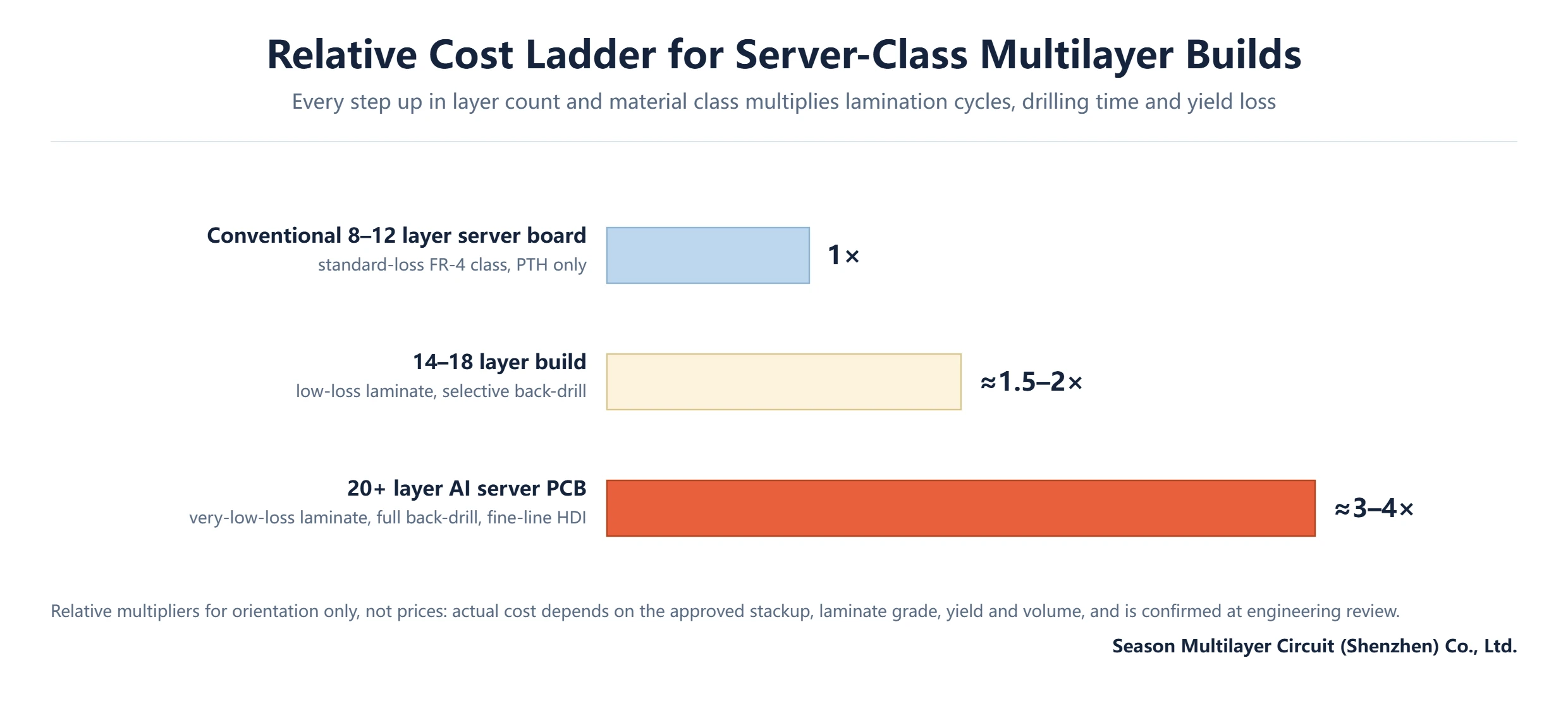
The premium over a conventional server board is additive across four independent drivers. None of them is optional once the interconnect budget is fixed, which is why value engineering on AI-class builds usually fails unless it reopens the stackup itself.
- Laminate class. Stepping from a standard-loss FR-4 grade to a very-low-loss grade multiplies the raw material cost per panel several times over, and thick multilayer panels consume more of it.
- Layer count and lamination cycles. Every additional press adds lamination time, drilling steps and registration risk, so cost climbs faster than linearly with layer count.
- Via operations. Back-drilling, resin plugging and copper capping each add dedicated process steps that a conventional board never runs.
- Yield. Fine-line, heavy-layer builds carry more scrappable value per panel and a longer detection chain, so immature stackups show visibly lower first-pass yield that gets priced in.
As a planning range, a 20-plus layer very-low-loss build with full back-drilling commonly lands at roughly three to four times the unit cost of a conventional 8–12 layer server board, and a 14–18 layer build with a low-loss grade sits at roughly 1.5 to 2 times. These are relative multipliers for budgeting conversations, not prices; the actual figure depends on the approved stackup and is confirmed at engineering review.
Impedance Control and Testing on AI Builds
A conventional board order usually specifies impedance on a handful of buses with a ±10% tolerance. An AI server PCB order specifies it on hundreds of differential pairs, with ±8% as the working norm and ±5% reserved for the most marginal lanes in the fabric. The tighter windows are achievable, but they consume engineering attention: the fabricator has to model with the right Dk, hold etch line-width control, and verify with coupons.
Verification is coupon-based. Test coupons built on the same panel carry the same stackup and trace geometry, and time-domain reflectometry readings are logged per production lot. Our impedance measurement guide explains how coupon placement and lot sampling work, so you can align the acceptance criteria in your quality plan with what the line actually tests.
Design Handoff Checklist Before You Request a Quote
Incomplete data packages are the most common reason AI-class quotes come back slow or padded. Before sending the package out, close the following items:
- Exported fabrication data in a standard format; the Gerber specification is maintained by Ucamco, and Gerber data with an accompanying drill file remains the safest exchange format for a first quote.
- A stackup intent sheet with layer count, dielectric targets, copper weights and the target material class, leaving brand alternates open for quoting.
- An impedance table listing every controlled pair with its tolerance band, so the fabricator can flag lanes that need ±5% instead of ±8%.
- A via table that marks which through-vias are back-drilled and from which side, plus any plugged or filled vias under BGAs.
- Board thickness and warpage allowance at assembly temperature, which matters at these thicknesses.
Packages that arrive with these five items typically go from quote request to engineering response in a single pass, because the fabricator does not need to guess the intent behind any layer.
Choosing a Manufacturer for AI-Class Builds
The eligible supplier pool narrows quickly at this complexity. Look for demonstrated volume capability at 20+ layers, laser microvia capability with 1-stage and 2-stage HDI, back-drilling and resin plugging in the standard process chain, and a quality system audited against IPC-A-600 Class 2 and Class 3 acceptance criteria, which the IPC standards framework sits under. Registration and traceability discipline matter as much as the headline capabilities, because every extra layer multiplies the cost of a misaligned one.
Season Multilayer Circuit produces rigid multilayer boards from 2 to 30 layers in volume, with 2/2 mil trace and space in production, 0.1 mm laser blind vias, resin plugging with copper capping, and back-drilling in the standard flow. For a worked example of how a dense interconnect board routes these decisions, see our 12-layer high-speed backplane PCB case, and for the full process chain from panel to shipment see the PCB manufacturing process overview. The manufacturing services page lists the capability envelope in RFQ-ready form.
Frequently Asked Questions
How many layers does an AI server PCB need?
Conventional server motherboards run 6 to 16 layers. Boards inside AI clusters — accelerator carrier boards, switch boards, line cards and backplanes — typically specify 20 to 30 layers because large BGA breakout plus dedicated reference planes for every high-speed lane consume routing resources quickly. Switch fabric boards can go higher still.
Why does an AI server PCB cost more than a conventional server board?
Four drivers stack up: the very-low-loss laminate class, the extra lamination cycles and drilling steps that 20+ layers require, dedicated via operations such as back-drilling and resin plugging, and the yield impact of fine-line heavy builds. In relative terms a 20+ layer build commonly lands at roughly 3–4× the unit cost of a conventional 8–12 layer server board, confirmed case by case at engineering review.
What laminate materials are used for AI server PCB builds?
Very-low-loss laminate grades with a dissipation factor at or below about 0.005 at 10 GHz are the working specification for PCIe Gen5-class and 56G PAM4 lanes. Specifying the class band in the RFQ rather than a single brand lets suppliers quote alternates with equivalent electrical performance, which usually improves both availability and pricing.
Does an AI server PCB always need HDI microvias?
Not always. Backplane-style boards often achieve breakout with back-drilled through-vias alone. HDI enters when fine-pitch BGAs on accelerator modules cannot escape on through-via geometry — 1-stage or 2-stage builds with laser microvias solve the fanout, and resin-plugged, copper-capped vias flatten pads where modules land directly on vias.
What impedance tolerances apply to AI server PCB differential pairs?
±10% remains the conventional default, but AI-class fabric lanes are usually specified at ±8%, with ±5% reserved for the most marginal pairs. The tighter window is verified with test coupons built on the same panel and measured by time-domain reflectometry per production lot, so put the tolerance band per lane in the impedance table of your data package.
Is back-drilling really necessary on high-layer-count server boards?
For high-speed lanes passing through inner layers, yes in practice: the unused through-via stub below the connected layer resonates at lane frequencies and erodes the channel margin that SerDes budgets depend on. Back-drilling removes most of the stub cheaply; the alternative is laser microvias throughout, which costs more, or limiting lane lengths, which the layout rarely allows.
How do I get a quote for an AI server PCB?
Send the Gerber package, a stackup intent with the target material class, an impedance table with per-lane tolerances and a via table marking back-drilled and plugged holes. The engineering review confirms the stackup, flags lanes that need tighter tolerance and returns a manufacturability read with the quote, which avoids the most common requote loops.
Get Your AI Server PCB Stackup Reviewed Before You Commit
Submit your Gerber data and stackup intent for an engineering review before release: the review confirms the layer-balance strategy, the via recipe including back-drill depth and plugged regions, and the impedance plan against ±8% and ±5% windows in one pass. If the design is still in floorplanning, the team can propose a reference stackup that keeps more fabricators eligible for the volume quote.