Book Appointment Now

How a 2-layer vs 4-layer PCB build differs in stackup, return path, impedance control, routing density and cost, with three questions that settle the choice.
2-Layer vs 4-Layer PCB: Structure, Performance and Cost Compared
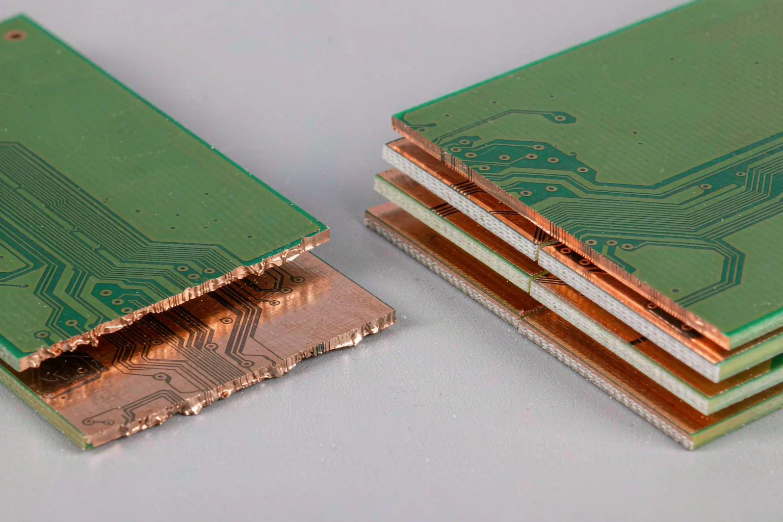
The same circuit can often be built on a two-layer board or on a four-layer board, and the quotations differ enough that the choice becomes a project decision. The real gap between a 2-layer vs 4-layer PCB build is not the layer count itself. It is what the two extra inner planes do to the return path, the impedance budget, the routing density and, downstream, the cost and lead time.
This guide compares the two structures side by side: stackup and inner planes first, then electrical performance, then routing density, then cost drivers and lead time, and finally three questions that settle which build your project actually needs. Every claim is written from a manufacturer’s engineering-review perspective, so you can reuse the tables directly in your own design review.
Table of Contents
- What Actually Changes Between Two and Four Layers
- Stackup and Inner-Plane Structure Compared
- Return Path and Signal Integrity: 2-Layer vs 4-Layer PCB
- Impedance Control Differences
- Routing Density and Component Placement
- Cost and Lead Time: The Honest Gap
- Copper Weight and Current Handling
- When a Two-Layer Board Is Still the Right Call
- When You Should Move to Four Layers
- Three Questions That Settle the 2-Layer vs 4-Layer PCB Choice
- FAQ
- Send Your Gerber for a Two-Layer vs Four-Layer Review
What Actually Changes Between Two and Four Layers
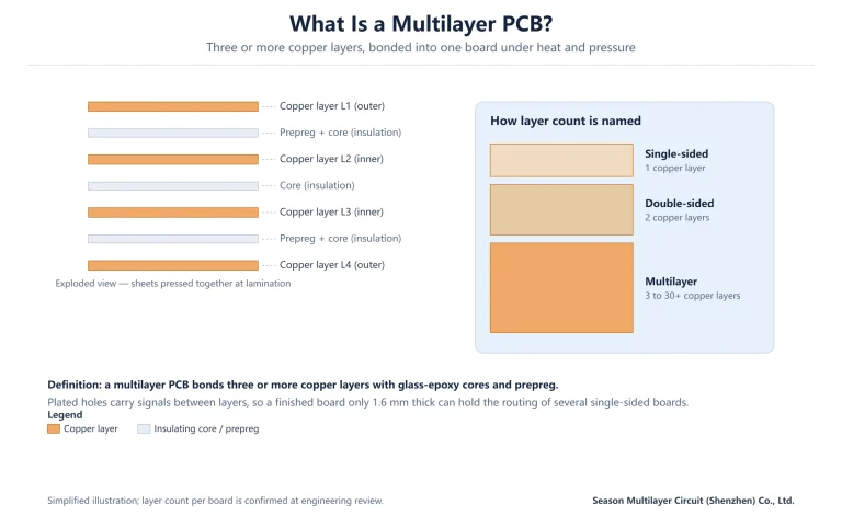
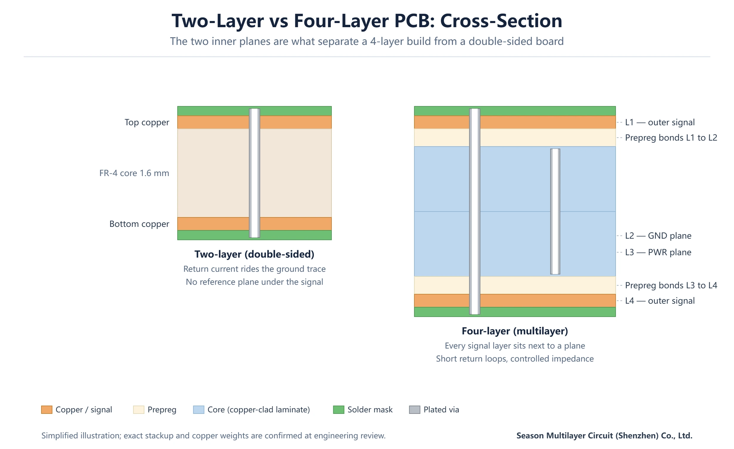
A two-layer board — usually called double-sided — has copper on the top and bottom faces of a single FR-4 core, connected by plated through holes. A four-layer board adds two inner copper layers: a typical stackup runs TOP / GND / PWR / BOT, with the ground and power planes buried inside the board and every signal layer sitting directly against a plane.
That is the structural heart of the 2-layer vs 4-layer PCB question: the inner planes take power and ground distribution off the outer routing layers. On a two-layer board, ground and power traces compete with signals for the same two copper layers; on a four-layer board, the outer layers are free for signals and the planes do the quiet work underneath. If you are new to the terminology, the multilayer PCB explainer covers how layer counts are named and bonded.
One practical note before the comparisons: a four-layer stackup does not have to be exotic. Standard builds cover most thickness and impedance targets, and customised stackups are only quoted when a design specifically calls for one — which keeps cost and lead time predictable.
Stackup and Inner-Plane Structure Compared
The cross-section below shows both builds. The two-layer board is one core with copper on both faces; the four-layer board is two copper-clad cores pressed with prepreg so that the GND and PWR planes end up as complete, unbroken sheets of copper. The comparison table translates the drawing into review-ready numbers.
| Comparison item | Two-layer (double-sided) | Four-layer (multilayer) |
|---|---|---|
| Copper layers | 2 (TOP and BOT) | 4 (TOP / GND / PWR / BOT typical) |
| Inner planes | None | One full ground plane plus one power plane |
| Layer interconnect | Plated through holes only | Through holes, plus buried vias when the build calls for them |
| Lamination | Single core, no press cycle | One lamination cycle; HDI adds stages on top |
| Typical line and space | 3/3 mil and coarser works well | 3/3 mil standard; 2/2 mil in HDI volume production |
| Typical finished thickness | 0.8–1.6 mm | 0.8–1.6 mm at the same footprint |
Because the planes are solid copper, the four-layer build also spreads current and shields the outer signal layers. How thick each copper layer should be, and how the dielectrics are proportioned, follows the same rules described in the PCB stackup design guide.
Return Path and Signal Integrity: 2-Layer vs 4-Layer PCB
Every switching current needs a return path, and the return path is where the two builds diverge most. On a four-layer board, a signal on the top layer returns through the ground plane directly beneath it; the loop area is small, so crosstalk and radiated emissions stay low. On a two-layer board, the return current squeezes into ground traces, the loop grows, and the penalty rises as edge rates get faster.
This is why boards that look electrically simple on a schematic can still fail EMC testing on a two-layer build. Long parallel runs share return segments, ground bounce appears across connectors, and every added interface makes the ground network harder to keep quiet. The routing habits that cause these problems — and the fixes — are collected in the signal trace design rules.
Engineers sometimes rescue a two-layer design with a hatched ground fill or a gridded ground. Those tricks help at low speeds, but they cannot reproduce a solid plane, so treat them as mitigation, not as equivalence.
Impedance Control Differences
Controlled impedance needs a predictable reference, and only a plane provides one. With inner planes, a single-ended 50 ohm trace or a 90–100 ohm differential pair can be modelled, built and measured reliably. Our tolerance practice is plus or minus 8 percent for volume production and plus or minus 5 percent for prototypes and specially reviewed builds, with a TDR coupon made on every panel.
| Electrical item | Two-layer | Four-layer |
|---|---|---|
| Reference for signals | Ground traces or partial fills | Solid GND or PWR plane adjacent to every signal layer |
| Single-ended 50 ohm | Achievable in pockets, weakly held | Held across the board, production-tight tolerance |
| Differential pairs (90–100 ohm) | Fragile near connectors and splits | Stable along the full route |
| Typical tolerance practice | Best effort, per-panel review | ±8% volume, ±5% prototype and reviewed builds, TDR coupon per panel |
| EMC headroom | Loop area grows with every interface | Plane shielding keeps loops small |
How those tolerances are actually verified on the shop floor — TDR coupons, sample plans and reporting — is described in the impedance measurement guide. If your interfaces carry impedance targets, that document pairs with this one when you write the fabrication drawing.
Routing Density and Component Placement
Density is the second dividing line. On a two-layer board, power and ground traces consume a meaningful share of both copper layers, and a design that does not fit is usually solved by growing the board. A four-layer board hands power and ground to the inner planes, so both outer layers route signals end to end, and the same circuit fits in less area with shorter nets.
The extra room also changes component placement. Fine-pitch parts want via escape routes, decoupling capacitors want short paths to a plane, and buses want to run without dodging ground traces. All of that becomes straightforward when planes absorb the power network. For highly compressed builds, the next step up is HDI; the HDI PCB technology guide explains how microvias and stacked stages add density on top of a four-layer floor.
Cost and Lead Time: The Honest Gap
Cost is where the 2-layer vs 4-layer PCB decision gets commercial. In relative terms, a four-layer board of the same size and quantity is commonly quoted at roughly two to three times the unit price of a comparable two-layer build, because it adds two inner-layer imaging cycles, a lamination press cycle, and more electrical test. Volume narrows the gap: batch pricing can fall to a fraction of prototype pricing as panel utilisation improves. The cost per square metre breakdown shows which variables move the number most.
Lead time follows the same logic. A two-layer board skips lamination and inner-layer processing, so its cycle is naturally shorter. A standard four-layer prototype slot typically runs about five working days at scheduling, with the exact date confirmed at engineering review rather than promised blind. Material choices amplify cost on both builds — mid-Tg and specialty dielectrics carry multipliers of their own, and surface finish selection (ENIG, OSP, HASL) moves the number again.
| Commercial item | Two-layer | Four-layer |
|---|---|---|
| Relative unit price (same size, same quantity) | Baseline | Roughly 2–3x, confirmed at engineering review |
| Batch effect | Volume discounts apply | Volume discounts apply, larger panel-utilisation benefit |
| Prototype cycle | Shortest (no lamination) | About 5 working days standard, confirmed at scheduling |
| Cost drivers | Size, copper weight, finish | Above plus inner-layer count and lamination |
| Typical uses | Consumer control boards, simple interfaces | Industrial, networking and any impedance-bearing design |
Copper Weight and Current Handling
Current handling interacts with the layer choice. At standard 1 oz copper, a 10 mm wide trace carries roughly 4–5 A as a conservative field value; 2 oz copper roughly doubles that, at a cost premium of around 20–40 percent. On a two-layer board the answer to a bigger load is almost always a wider trace, which consumes routing space you may not have.
On a four-layer board you have more options: put the high current on a plane, split the power island, or specify heavier copper on selected layers. For power-stage designs the heavy copper PCB guide sets out what 2 oz and beyond changes for etch, plating and cost.
When a Two-Layer Board Is Still the Right Call
Moving to four layers is not automatically the better engineering. Plenty of products ship on two layers for good reasons, and the honest list looks like this:
- The circuit is functionally simple: relays, sensors with slow outputs, LED drivers, basic power conversion.
- No interface carries an impedance target — no USB, Ethernet, DDR or RF sections with controlled-impedance notes on the drawing.
- Board area is cheap relative to the product, so routing that sprawls is acceptable.
- EMC exposure is mild: slow edge rates, enclosed enclosures, no radio next door.
- Unit cost pressure dominates and volumes are large, so every cent of board price matters.
If the design passes those filters, a disciplined two-layer layout with a solid ground strategy will serve reliably — and the factory accepts the build the same way as any other.
When You Should Move to Four Layers
Three situations flip the decision, and they cover most upgrades we see at engineering review:
- Impedance-bearing interfaces: USB, Ethernet, DDR, LVDS or any pair the drawing controls. A plane-referenced build holds the tolerance; a ground-trace build hopes.
- Density without room: the two-layer version only routes if the board grows, and the grown board costs more than the four-layer one that stays compact.
- EMC requirements with teeth: conducted or radiated limits that a trace-based return path repeatedly fails, where plane shielding fixes the loop area once.
Layer count is one input to the balanced stackup and warpage control discussion too — symmetric copper distribution matters more as boards thicken, and a four-layer build makes balance easy to arrange.
Three Questions That Settle the 2-Layer vs 4-Layer PCB Choice
Put the comparison into three questions and the decision usually makes itself:
- Does any net carry an impedance target? Yes means four layers from the start.
- Does the two-layer routing only fit by growing the board? A larger two-layer board often costs the same as a compact four-layer one, so compare quotes at equal function, not equal size.
- How strict are the EMC and interface requirements? Strict means planes; planes mean four layers.
For the fabrication side, acceptance follows IPC Class 2 by default with Class 3 on request, and routine inspection runs 100 percent electrical test plus AOI, with X-ray sampling on BGA lots. Both builds ship under the same quality system, so the choice stays an engineering and cost decision, not a quality one. Reference designs that made each call are documented on our 4-layer SATA SSD PCB and 4-layer automotive PCB pages.
Frequently Asked Questions
What is the difference between a 2-layer and a 4-layer PCB?
Structurally, a four-layer board adds two inner copper planes — typically GND and PWR — between the outer signal layers, bonded with prepreg. Electrically that shortens the return path, makes controlled impedance reliable and frees both outer layers for signals. Commercially it adds inner-layer imaging and a lamination cycle, so the unit price runs roughly two to three times a comparable two-layer build.
Can a 2-layer board replace a 4-layer design?
Sometimes. If the circuit has no impedance-bearing interfaces, routes without growing the board, and faces mild EMC requirements, a disciplined two-layer layout is a legitimate choice. Once USB, Ethernet, DDR or similar interfaces appear, or density forces the board to grow, the two-layer build loses on both performance and total cost.
How much more does a 4-layer PCB cost than a 2-layer board?
For the same size and quantity, expect a quotation of roughly two to three times the two-layer unit price, driven by two extra imaging cycles, a press cycle and wider electrical test. Volume production narrows the gap through better panel utilisation, and the exact ratio is confirmed at engineering review.
What goes on the inner layers of a 4-layer PCB?
The common arrangement is a full ground plane on layer 2 and a power plane on layer 3, so TOP and BOT route signals against clean references. Variants exist — split power planes, signal layers inside for extra routing — and the layer pair order is confirmed against the impedance and EMC requirements of the design.
When is a 4-layer PCB mandatory?
Three cases: interfaces with controlled impedance targets, designs that only fit if the board grows, and EMC limits that a trace-based return path cannot meet. Under any of the three, a four-layer build is usually cheaper overall than fighting the two-layer version.
Is a 4-layer PCB harder to manufacture than a 2-layer board?
It adds inner-layer imaging, oxide treatment and a lamination press, but for a qualified multilayer shop the process is routine and runs under the same IPC Class 2 acceptance criteria with 100 percent electrical test and AOI. Reliability differences come from stackup balance, not from layer count itself.
Should I jump from 2 layers straight to 6 layers?
Only if a four-layer build genuinely cannot carry the routing. A six-layer board adds two more signal layers and more plane options for dense high-speed designs, but each extra layer raises price and lead time. Review the stackup against impedance and density needs first; most upgrades settle comfortably at four.
Send Your Gerber for a Two-Layer vs Four-Layer Review
Unsure which build your project deserves? Submit the Gerber data and impedance notes through our PCB manufacturing services page, and the engineering team will return a concrete comparison — stackup options, impedance tolerance, routing density and relative cost — so you can decide on numbers instead of instinct. Design data stays confidential and is used only for the review.