Book Appointment Now

A process-level tour of outer layer PCB fabrication, from copper prep and dry film imaging to pattern plating, etch control and final AOI.
Outer Layer PCB Fabrication: Pattern Plating to Final Etch
Outer layers carry the interfaces a board actually presents to the world — connectors, RF pads, BGA fanouts, test points — and they are where signal integrity, plating quality and yield meet. This guide walks through outer layer PCB fabrication the way a process engineer sees it: copper preparation, dry film imaging, pattern plating, etch control, and the inspections that hold line width in specification.
Every number below is a control window from the line or a relative comparison; the exact values for your build are confirmed at engineering review. If your design uses microvias, pair it with the HDI technology guide — the build-up structure changes what the outer layers have to deliver.
Table of Contents
- Outer Layer PCB Fabrication at a Glance
- Surface Preparation: Where Adhesion Is Won
- Dry Film Imaging: Exposure and Development Windows
- Pattern Plating: Copper Only Where Traces Belong
- Pattern vs Panel Plating in Outer Layer PCB Fabrication
- Etch Control, Side Etch and Etch Factor
- High Aspect Ratio Holes and Microvias at the Outer Layers
- Inspection: AOI, Impedance and Cross-Section
- Greener and Data-Driven: Where Outer Layers Are Heading
- FAQ
- Have Your Outer Layer Stackup Reviewed
Outer Layer PCB Fabrication at a Glance
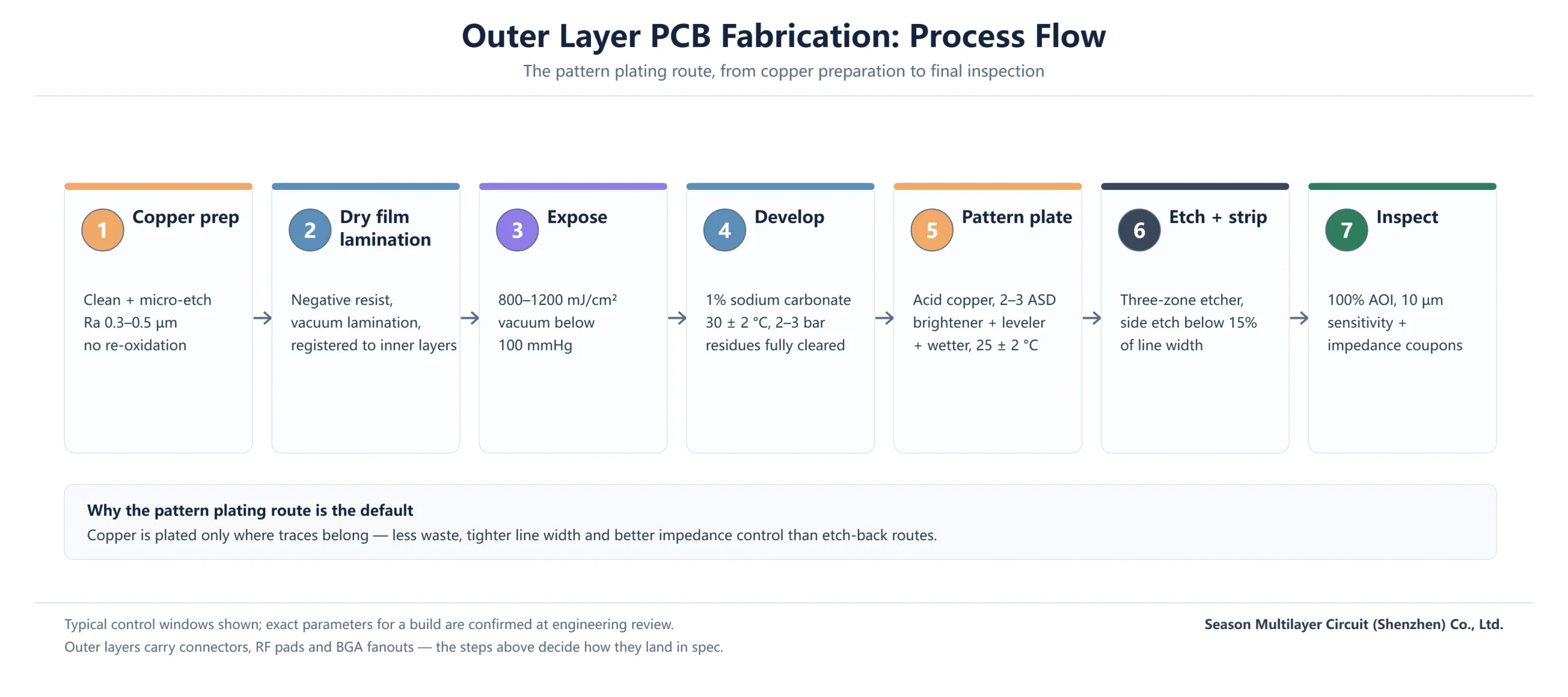
Seven steps take a panel from laminate to inspected outer circuitry: copper preparation, dry film lamination, exposure, development, pattern plating, etching with resist stripping, then inspection. The route is called pattern plating because copper is grown only where traces belong — the alternative, plating the whole panel and etching most of it away, survives only in niches. Table 1 maps the sequence and the controls each step owns.
| Step | Purpose | Key controls |
|---|---|---|
| 1. Copper prep | Remove oxide and set adhesion roughness | Micro-etch depth, rinse quality, time to lamination |
| 2. Dry film lamination | Apply negative photoimageable resist | Roll temperature, speed, pressure, layer registration |
| 3. Expose | Transfer artwork into the resist | Exposure energy, vacuum contact, artwork alignment |
| 4. Develop | Clear the areas that must not remain | Solution strength, temperature, spray pressure |
| 5. Pattern plate | Grow copper where traces belong | Current density, bath chemistry, additive balance |
| 6. Etch + strip | Remove unprotected copper, retire the resist | Etchant chemistry, three-zone profile, strip cleanliness |
| 7. Inspect | Hold the result to specification | 100% AOI, impedance coupons, cross-section |
Seen from the design side, the sequence turns your Gerber data into copper geometry with three deliverables in tension: line width and spacing, copper thickness in traces and holes, and the impedance classes those geometries must hit. A well-run outer layer PCB fabrication line holds all three at once — and an 8-layer security system PCB shows the discipline at standard class just as clearly as an HDI prototype does at fine pitch.
Surface Preparation: Where Adhesion Is Won
Adhesion is decided before the resist ever touches the panel. Chemical cleaning removes the oxide that copper regrows within minutes; a micro-etch then roughens the surface to a controlled roughness in the 0.3–0.5 µm band, where dry film grip is strongest. Too smooth and the resist lifts during plating; too rough and fine-line definition suffers at the edges. The IPC standards set the acceptance language for the surface and finish conditions this step has to reach.
The clock matters as much as the chemistry. Prepared panels move to lamination immediately, because a cleaned copper surface begins re-oxidizing on contact with air — and every hour of delay shows up later as adhesion loss and resist wraps. Incoming material gets its own gates: copper foil thickness within ±3%, surface roughness below 0.5 µm, and laminate dimensional stability better than 0.1%, so inner-layer registration survives outer-layer handling.
Dry Film Imaging: Exposure and Development Windows
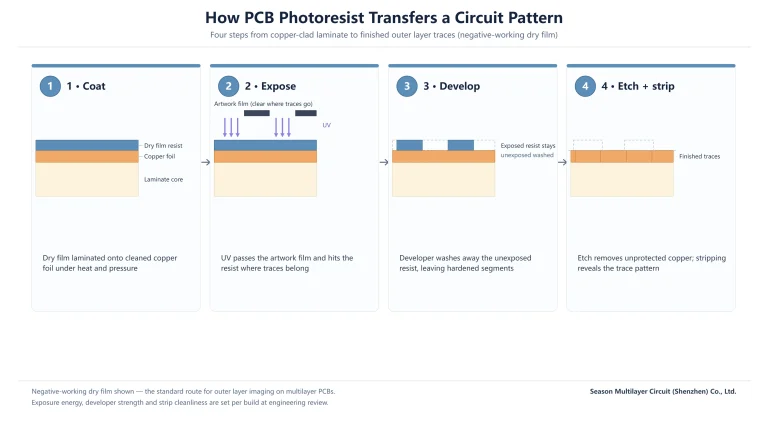
Modern outer layer imaging uses negative-working dry film. Exposure energy sits in the 800–1200 mJ/cm² band, with vacuum pulled below 100 mmHg so the artwork film sits against the resist without an air gap — that contact is what keeps line edges vertical instead of shadowed. Development then clears the unexposed areas in a 1% sodium carbonate solution at 30 ± 2 °C under 2–3 bar spray pressure, strong enough to remove film cleanly without eroding the pattern it must keep.
The windows are narrow on purpose. Underexposure leaves the resist under-crosslinked, and development attacks it; overexposure fattens the artwork and closes fine gaps. Registration to the inner layers is verified before exposure is released, because outer layers have to land on the buried structure, not just on themselves.
Pattern Plating: Copper Only Where Traces Belong
Pattern plating runs an acid sulfate copper bath with three organic additives in balance: a brightener that keeps the deposit dense and fine-grained, a leveler that evens thickness between high and low current density areas, and a wetter that helps solution reach tight geometry. Current density runs 2–3 ASD with the bath held at 25 ± 2 °C and continuously filtered.
The targets are thickness where the design needs it and uniformity across the panel — plating uniformity above 85% is the process control gate — because every variance here becomes an impedance variance later. The Gerber data defines where copper may grow; the bath defines how evenly it does. Hole walls depend on the same discipline, and the high-aspect-ratio techniques later in this article extend it down the barrel of small vias.
When the balance drifts, the board tells on itself: burned deposits at high-current-density corners, dull or nodular copper in low-flow areas, thickness drift between holes and traces. Scheduled bath analysis keeps the additive triangle honest — and it is part of the document trail a buyer can request with any first-article report.
Pattern vs Panel Plating in Outer Layer PCB Fabrication
Panel plating — plate everything, then etch the pattern — still exists in simple, low-density work, and comparing the two shows why pattern plating became the default for anything dense. Etching back a fully plated surface wastes 40–50% of the copper as dissolved scrap and consumes proportionally more etchant and waste treatment capacity.
The geometry cost is worse than the material cost. When features shrink below about 50 µm, the panel route’s side etch reaches 25–35% of the design line width — traces emerge trapezoidal and marginal. Cycle time stretches by a quarter or more, and yield in that route typically drops around fifteen points. In outer layer PCB fabrication, pattern plating keeps the copper, the geometry and the schedule.
| Aspect | Pattern plating | Panel plating |
|---|---|---|
| Copper utilization | Plated only where traces belong | 40–50% etched away as scrap |
| Fine-line geometry | Side etch contained by etch-factor control | Side etch reaches 25–35% of line width below 50 µm |
| Cycle time | Shorter — no full-surface etch back | Around 25% longer |
| Yield tendency | Standard for dense multilayer builds | Typically around 15 points lower in comparable work |
| Where it survives | Almost everything from prototype to production | Simple, low-density panels |
Etch Control, Side Etch and Etch Factor
Etching shapes the final trace, and it attacks sideways as well as down. Etch factor — conductor thickness divided by horizontal side etch — is the number that captures the damage: at 1:1 the undercut under the resist edge equals the copper thickness, leaving a strongly trapezoidal trace that drifts from both the designed width and the impedance model.
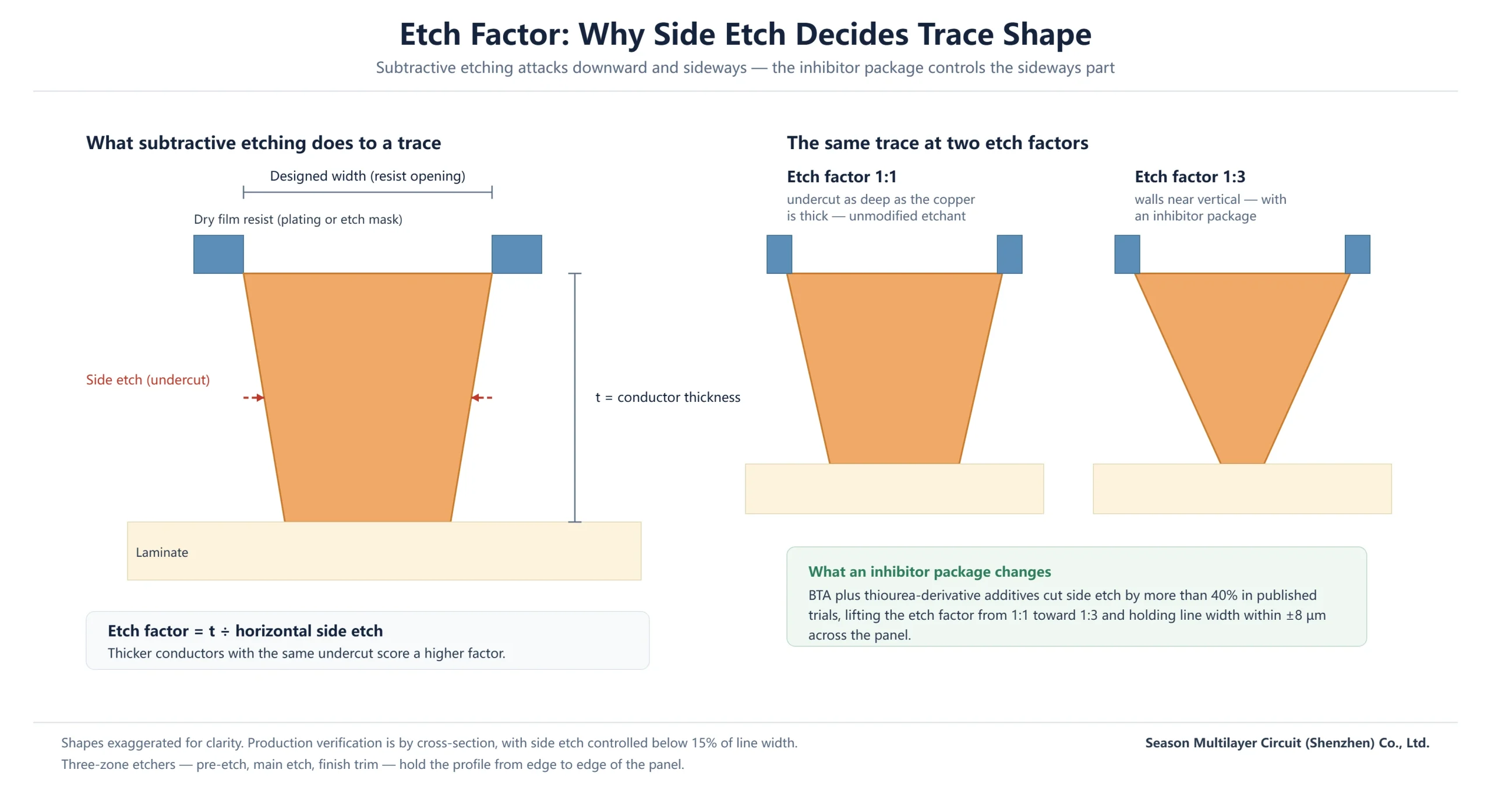
Chemistry fights back. Additive packages built on benzotriazole (0.5–1.5%) plus thiourea derivatives (0.1–0.3%) cut side etch by more than 40% in published trials, lifting etch factor from 1:1 toward 1:3. Equipment does the rest: modern etchers run three zones — a gentle pre-etch start, a full-strength main etch, and a finishing trim — holding line width within ±8 µm across the panel, while laser thickness gauges and automatic chemistry dosing lift etch uniformity by around 30% and reduce over-etch risk.
The production gate a buyer can ask about: side etch held below 15% of line width, verified by cross-section. Combined with the inhibitor chemistry, that is what keeps a 4 mil trace from becoming a 3 mil trace with an impedance surprise.
High Aspect Ratio Holes and Microvias at the Outer Layers
High-speed designs push vias from aspect ratio 3:1 toward 5:1, and plating chemistry alone cannot keep the barrel uniform at that depth. Pulse plating replaces direct current with controlled on-off cycles, and the measured effect is large: hole copper uniformity improves from about 65% to 85% on high-aspect-ratio holes.
Fine outer features change the resist side too: liquid photoimageable resists take over below roughly 50 µm, where dry film resolution runs out. On the drilling side, CO₂ laser systems running high-frequency pulses (5–10 kHz) with beam shaping produce 50–100 µm microvias at ±10 µm placement accuracy, while UV laser drilling reaches 20–50 µm with cleaner hole walls. Direct metallization — nanoscale carbon or conductive polymer seed layers — replaces electroless copper for hole coverage, removing a formaldehyde-bearing chemistry step in the process.
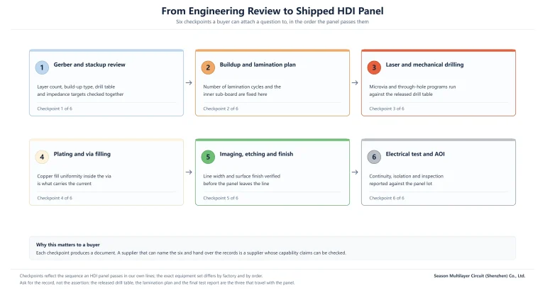
These outer-layer techniques are the visible half of HDI work. The HDI PCB technology guide explains how the build-up underneath is structured, the 1-stage vs 2-stage vs 3-stage comparison shows how stacking choices change the lamination plan, and the 10-layer 2-stage HDI prototype shows the resulting stackup with its capability numbers released.
Inspection: AOI, Impedance and Cross-Section
Final quality is a gate, not a hope. Automated optical inspection screens 100% of outer layers with defect sensitivity at 10 µm; impedance coupons ride the panel and are tested against the class the build commits to — commonly ±8% for high-speed work, within the ±10%, ±8% and ±5% classes we offer. Where the design justifies it, cross-sections verify side etch, plating thickness and hole copper directly.
Advanced verification goes further when the application demands it: white-light interferometry or laser confocal microscopy profiles trace geometry in three dimensions, thermomechanical analysis checks how the finished circuit’s materials expand together through temperature cycling, and vector network analyzers confirm insertion and return loss on high-frequency builds. UL Solutions recognition on the laminate system is checked against the same stackup at the same time. Table 3 collects the control points a buyer can audit.
| Checkpoint | Parameter | Typical limit |
|---|---|---|
| Incoming copper foil | Thickness tolerance | ±3% |
| Incoming copper foil | Surface roughness | Below 0.5 µm |
| Laminate | Dimensional stability | Better than 0.1% |
| Pattern plating | Plating uniformity | Above 85% |
| Etching | Side etch | Below 15% of line width |
| Etching zone control | Line width accuracy | ±8 µm |
| Final inspection | AOI coverage and sensitivity | 100% at 10 µm |
| Final inspection | Impedance tolerance | Class dependent: ±10%, ±8% or ±5% |
Greener and Data-Driven: Where Outer Layers Are Heading
Two currents are reshaping outer layer work. Additive manufacturing is arriving in earnest: inkjet systems with nano-copper conductive inks now write 15–20 µm traces directly, cutting material consumption by more than 70% against subtractive routes, while laser-induced activation turns insulation into circuit selectively — a natural fit for three-dimensional structures.
Sustainability pressure is rewriting the chemistry shelves: halogen-free laminates, finishes compliant with RoHS, water-based cleaning agents and biodegradable process chemicals. Metal recovery closes the loop — electrolytic copper and tin recovery above 95%, with water reuse above 80% — and it is becoming a procurement question, not just an environmental one.
The data layer ties it together. Digital twins map production parameters in real time — early deployments report roughly 20% throughput gains and 30% fewer defects — and AI-based inspection classifies defects and traces root causes at better than 95% accuracy. For buyers, the practical takeaway is to ask which of these systems a supplier actually runs, because the answers separate the lines that hold tolerance from the lines that chase it.
Frequently Asked Questions
What is outer layer PCB fabrication?
It is the sequence that forms the circuitry on a board’s outer layers: copper preparation, dry film lamination, artwork exposure, development, pattern plating of copper, etching with resist stripping, and inspection. The pattern plating route is the industry default because it wastes less copper, holds line width tighter and supports controlled impedance.
Why is pattern plating preferred over panel plating?
Panel plating plates the whole surface and etches most of it away, wasting 40–50% of the copper and stretching cycle time by a quarter or more. Below roughly 50 µm features its side etch reaches 25–35% of the line width, and yield typically drops around fifteen points. Pattern plating grows copper only where traces belong.
What is etch factor in PCB manufacturing?
Etch factor is conductor thickness divided by horizontal side etch. Unmodified etchant gives roughly 1:1, meaning the undercut under the resist edge equals the copper thickness. Inhibitor chemistry lifts the ratio toward 1:3, keeping walls near vertical, holding line width within ±8 µm and protecting the impedance model.
How much does side etch affect finished trace width?
Well-controlled subtractive etching holds side etch below 15% of line width, verified by cross-section. Above that gate, traces narrow, impedance shifts, and fine-pitch features become marginal. Panel-plated routes are the most exposed, with side etch of 25–35% of line width on features below 50 µm.
What impedance tolerance can outer layers hold?
We commit to ±10%, ±8% or ±5% by build class, with ±8% common on high-speed work. Tolerance is earned upstream — surface preparation, imaging resolution, plating uniformity and etch factor all feed the final geometry — which is why impedance coupons ride the panel and are tested before shipment.
How are PCB outer layers inspected?
Automated optical inspection screens 100% of outer layers at 10 µm defect sensitivity, impedance coupons are tested against the build class, and cross-sections verify side etch, trace geometry and plating thickness. High-reliability builds add white-light interferometry for 3D trace profiling and vector network analyzer measurement of insertion and return loss.
How do microvias change outer layer fabrication?
They add laser drilling — CO₂ systems produce 50–100 µm microvias at ±10 µm placement accuracy, and UV laser reaches 20–50 µm — plus direct metallization seed layers and pulse plating for high-aspect-ratio holes. Liquid photoimageable resists take over imaging below about 50 µm, delivering fine-pitch fanout the mechanical drill route cannot.
Have Your Outer Layer Stackup Reviewed
Send your Gerber package, drill table and impedance targets through engineering review before committing a build. The review confirms the imaging and plating route, flags geometry that stresses the etch window, and returns a stackup proposal with the tolerance classes you can hold us to — prototype through production, 2–30 layers.
Start at our PCB manufacturing services page, or compare a released example in the 10-layer HDI industrial control PCB.